DSP_算法综合与优化(英文书)

摘要:
本书是 DSP 算法综合与优化的权威专著,聚焦数字信号处理算法的硬件自动化实现与多字长优化技术。全书系统讲解信号峰值估计、字长优化、饱和运算、调度与资源绑定等核心内容,提出多字长设计范式,结合解析模型与启发式算法,在满足精度约束下最小化硬件面积、功耗并提升速度。书中覆盖线性 / 非线性系统、自适应滤波、IIR/FIR 滤波器等典型应用,给出基于 MILP 的最优求解与高效启发式方案,支持 FPGA/ASIC 平台实现。通过饱和运算与架构协同优化,显著降低资源占用,为 DSP 算法硬件化设计提供完整理论、方法与工程实践参考。
SYNTHESIS AND OPTIMIZATION OF DSP ALGORITHMS
This page intentionally left blank
by
George A. Constantinides
Imperial College, London
Peter Y.K. Cheung
Imperial College, London
and
Wayne Luk
Imperial College, London
KLUWER ACADEMIC PUBLISHERS
NEW YORK, BOSTON, DORDRECHT, LONDON, MOSCOW
eBook ISBN: 1-4020-7931-1
Print ISBN: 1-4020-7930-3
©2004 Kluwer Academic Publishers
New York, Boston, Dordrecht, London, Moscow
Print ©2004 Kluwer Academic Publishers Dordrecht
All rights reserved
No part of this eBook may be reproduced or trans mitted in any form or by any means, electronic, mechanical, recording, or otherwise, without written consent from the Publisher
Created in the United States of America
Visit Kluwer Online at: http://kluweronline.com
and Kluwer's eBookstore at: http://ebooks.kluweronline.com
This page intentionally left blank
Preface
Digital signal processing (DSP) has undergone an immense expansion since the foundations of the subject were laid in the 1970s. New application areas have arisen, and DSP technology is now essential to a bewildering array of fields such as computer vision, instrumentation and control, data compression, speech recognition and synthesis, digital audio and cameras, mobile telephony, echo cancellation, and even active suspension in the automotive industry.
In parallel to, and intimately linked with, the growth in application areas has been the growth in raw computational power available to implement DSP algorithms. Moore’s law continues to hold in the semiconductor industry, res- ulting every 18 months in a doubling of the number of computations we can perform.
Despite the rapidly increasing performance of microprocessors, the compu- tational demands of many DSP algorithms continue to outstrip the available computational power. As a result, many custom hardware implementations of DSP algorithms are produced - a time consuming and complex process, which the techniques described in this book aim, at least partially, to automate.
This book provides an overview of recent research on hardware synthesis an optimization of custom hardware implementations of digital signal processors. It focuses on techniques for automating the production of area-efficient designs from a high-level description, while satisfying user-specified constraints. Such techniques are shown to be applicable to both linear and nonlinear systems: from finite impulse response (FIR) and infinite impulse response (IIR) filters to designs for discrete cosine transform (DCT), polyphase filter banks, and adaptive least mean square (LMS) filters.
This book is designed for those working near the interface of DSP al- gorithm design and DSP implementation. It is our contention that this inter- face is a very exciting place to be, and we hope this book may help to draw the reader nearer to it.
London, George A. Constantinides
February 2004 Peter Y.K. Cheung
Wayne Luk
1 Introduction
1.1 Objectives
This book addresses the problem of hardware synthesis from an initial, in- finite precision, specification of a digital signal processing (DSP) algorithm. DSP algorithm development is often initially performed without regard to fi- nite precision effects, whereas in digital systems values must be represented to a finite precision [Mit98]. Finite precision representations can lead to undesir- able effects such as overflow errors and quantization errors (due to roundoff or truncation). This book describes methods to automate the translation from an infinite precision specification, together with bounds on acceptable errors, to a structural description which may be directly implemented in hardware. By automating this step, raise the level of abstraction at which a DSP algorithm can be specified for hardware synthesis.
We shall argue that, often, the most efficient hardware implementation of an algorithm is one in which a wide variety of finite precision representations of different sizes are used for different internal variables. The size of the rep- resentation of a finite precision ζword’ is referred to as its word-length. Imple- mentations utilizing several different word-lengths are referred to as ζmultiple word-length’ implementations and are discussed in detail in this book.
The accuracy observable at the outputs of a DSP system is a function of the word-lengths used to represent all intermediate variables in the algorithm. However, accuracy is less sensitive to some variables than to others, as is implementation area. It is demonstrated in this book that by considering error and area information in a structured way using an alytical and semi-an alytical noise models, it is possible to achieve highly efficient DSP implementations.Multiple word-length implementations have recently become a flourishing area of research [KWCM98, WP98, CRS+ 99, SBA00, BP00, KS01, NHCB01]. Stephenson [Ste00] enumerates three target areas for this research: SIMD architectures for multimedia [PW96], power conservation in embedded sys- tems [BM99], and direct hardware implementations. Of these areas, this book targets the latter, although Chapters 3 to 5 could form the basis of an ap- proach to the first two application areas.
Throughout the book, both the word-length of operations, and the overflow methods used, are considered to be optimization variables for minimizing the area or power consumption of a hardware implementation. At the same time, they impost constraints on possible solutions on the basis of signal quality at the system outputs. The resulting multiple word-length implementations pose new challenges to the area of high-level synthesis [Cam90], which are also addressed in this book.
1.2 Overview
The overall design flow proposed and discussed is illustrated in Fig. 1.1. Each of the blocks in this diagram will be discussed in more detail in the chapters to follow.
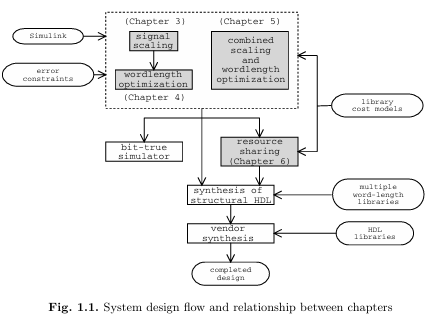
We begin in Chapter 2 by reviewing some relevant backgroud material, including a very brief introduction to important nomenclature in DSP, digital design, and algorithm representation. The key idea here is that in an efficient hardware implementation of a DSP algorithm, the representation used for each signal can be different from that used for other signals. Our representation consists of two parts: the scaling and the word-length. The optimization of these two parts are covered respectively in Chapters 3 and 4.
Chapter 3 reviews approaches to determining the peak signal value in a sig- nal processing system, a fundamental problem when selecting an appropriate fixed precision representation for signals.
Chapter 4 introduces and formalizes the idea of a multiple word-length im- plementation. An ana lytic noise model is described for the modelling of signal truncation noise. Techniques are then introduced to optimize the word-lengths of the variables in an algorithm in order to achieve a minimal implementation area while satisfying constraints on output signal quality. After an an alysis of the nature of the constraint space in such an optimization, we introduce a heuristic algorithm to address this problem. An extension to the method is presented for nonlinear systems containing differentiable nonlinear com- ponents, and results are presented illustrating the advantages of the methods described for area, speed, and power consumption.
Chapter 5 continues the above discussion, widening the scope to include the ability to predict the severity of overflow-induced errors. This is exploited by the proposed combined word-length and scaling optimization algorithm in order to automate the design of saturation arithmetic systems.
Chapter 6 addresses the implications of the proposed multiple word-length scheme for the problem of architectural synthesis. The chapter starts by high- lighting the differences between architectural synthesis for multiple word- length systems and the standard architectural synthesis problems of schedul- ing, resource allocation, and resource binding. Two methods to allow the shar- ing of arithmetic resources between multiple word-length operations are then proposed, one optimal and one heuristic.
Notation will be introduced in the book as required. For convenience, some basic notations required throughout the book are provided in Appendix A, p. 151. Some of the technical terms used in the book are also described in the glossary, p. 153. In addition, it should be noted that for ease of reading the box symbol: u∩ is used throughout this book to denote the end of an example, definition, problem, or claim.
2 Background
This chapter provides some of the necessary background required for the rest of this book. In particular, since this book is likely to be of interest both to DSP engineers and digital designers, a basic introduction to the essential nomenclature within each of these fields is provided, with references to further material as required.
Section 2.1 introduces microprocessors and field-programmable gate ar- rays. Section 2.2 then covers the discrete-time description of signals using the ≈-transform. Finally, Section 2.3 presents the representation of DSP al- gorithms using computation graphs.
2.1 Digital Design for DSP Engineers
2.1.1 Microprocessors vs. Digital Design
One of the first options faced by the designer of a digital signal processing system is whether that system should be implemented in hardware or soft- ware. A software implementation forms an attractive possibility, due to the mature state of compiler technology, and the number of good software en- gineers available. In addition microprocessors are mass-produced devices and therefore tend to be reasonably inexpensive. A major drawback of a micro- processor implementation of DSP algorithms is the computational throughput achievable. Many DSP algorithms are highly parallelizable, and could benefit significantly from more fine-grain parallelis m than that available with gen- eral purpose microprocessors. In response to this acknowledged drawback, general purpose microprocessor manufacturers have introduced extra single- instruction multiple-data (SIMD) instructions targetting DSP such as the Intel MMX instruction set [PW96] and Sun’s VIS instruction set [TONH96]. In addition, there are microprocessors specialized entirely for DSP such as the well-known Texas Instruments DSPs [TI]. Both of these implementations al- low higher throughput than that achievable with a general purpose processor, but there is still a significant limit to the throughput achievable.
The alternative to a microprocessor implementation is to implement the algorithm in custom digital hardware. This approach brings dividends in the form of speed and power consumption, but suffers from a lack of mature high-level design tools. In digital design, the industrial state of the art is register-transfer level (RTL) synthesis [IEE99, DC]. This form of design in- volves explicitly specifying the cycle-by-cycle timing of the circuit and the word-length of each signal within the circuit. The architecture must then be encoded using a mixture of data path and finite state machine constructs. The approaches outlined in this book allow the production of RTL-synthesizable code directly from a specification format more suitable to the DSP application domain.
2.1.2 The Field-Programmable Gate Array
There are two main drawbacks to designing an application-specific integrated circuit (ASICs) for a DSP application: money and time. The production of state of the art ASICs is now a very expensive process, which can only real- istically be entertained if the market for the device can be counted in millions of units. In addition, ASICs need a very time consuming test process before manufacture, as ζbug fixes’ cannot be created easily, if at all.
The Field-Programmable Gate Array (FPGA) can overcome both these problems. The FPGA is a programmable hardware device. It is mass-produced, and therefore can be bought reasonably inexpensively, and its programmabil- ity allows testing in-situ. The FPGA can trace its roots from programmable logic devices (PLDs) such as PLAs and PALs, which have been readily avail- able since the 1980s. Originally, such devices were used to replace discrete logic series in order to minimize the number of discrete devices used on a printed circuit board. However the density of today’s FPGAs allows a single chip to replace several million gates [Xil03]. Under these circumstances, using FPGAs rather than ASICs for computation has become a reality.
There are a range of modern FPGA architectures on offer, consisting of several basic elements. All such architectures contain the 4-input lookup table (4LUT or simply LUT) as the basic logic element. By configuring the data held in each of these s mall LUTs, and by configuring the way in which they are connected, a general circuit can be implemented. More recently, there has been a move towards heterogeneous architectures: modern FPGA devices such as Xilinx Virtex also contain embedded RAM blocks within the array of LUTs, Virtex II adds discrete multiplier blocks, and Virtex II pro [Xil03] adds PowerPC processor cores.
Although many of the approaches described in this book can be applied equally to ASIC and FPGA-based designs, it is our belief that programmable logic design will continue to increase its share of the market in DSP applic- ations. For this reason, throughout this book, we have reported results from these methods when applied to FPGAs based on 4LUTs.
2.1.3 Arithmetic on FPGAs
Two arithmetic operations together dominate DSP algorithms: multiplication and addition. For this reason, we shall take the opportunity to consider how multiplication and addition are implemented in FPGA architectures. A basic understanding of the architectural issues involved in designing adders and multipliers is key to understanding the area models derived in later chapters of this book.
Many hardware architectures have been proposed in the past for fast ad- dition. As well as the simple ripple-carry approach, these include carry-look- ahead, conditional sum, carry-select, and carry-skip addition [Kor02]. While the ASIC designer typically has a wide choice of adder implementations, most modern FPGAs have been designed to support fast ripple-carry addition. This means that often, ζfast’ addition techniques are actually slower than ripple- carry in practice. For this reason, we restrict ourselves to ripple carry addition.
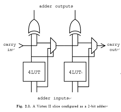
Fig. 2.1 shows a portion of the Virtex II ζslice’ [Xil03], the basic logic unit within the Virtex II FPGA. As well as containing two standard 4LUTs, the slice contains dedicated multiplexers and XOR gates. By using the LUT to generate the ζcarry propagate’ select signal of the multiplexer, a two-bit adder can be implemented within a single slice.
In hardware arithmetic design, it is usual to separate the two cases of multiplier design: when one operand is a constant, and when both operands may vary. In the former case, there are many opportunities for reducing the hardware cost and increasing the hardware speed compared to the latter case. A constant-coefficient multiplication can be re-coded as a sum of shifted ver- sions of the input, and common sub-expression elimination techniques can be applied to obtain an efficient implementation in terms of adders alone [Par99] (since shifting is free in hardware). General multiplication can be performed by adding partial products, and general multipliers essentially differ in the ways they accumulate such partial products. The Xilinx Virtex II slice, as well as containing a dedicated XOR gate for addition, also contains a dedic- ated AND gate, which can be used to calculate the partial products, allowing the 4LUTs in a slice to be used for their accumulation.
2.2 DSP for Digital Designers
A signal can be thought of as a variable that conveys information. Often a signal is one dimensional, such as speech, or two dimensional, such as an image. In modern communication and computation, such signals are often stored digitally. It is a common requirement to process such a signal in order to highlight or supress something of interest within it. For example, we may wish to remove noise from a speech signal, or we may wish to simply estimate the spectrum of that signal.
By convention, the value of a discrete-time signal x can be represented by a sequence x[n]. The index n corresponds to a multiple of the sampling period T , thus x[n] represents the value of the signal at time nT. The z transform (2.1) is a widely used tool in the an alysis and processing of such signals.

The z transform is a linear transform, since if X1 (z) is the transform of x1 [n] and X2 (z) is the transform of x2 [n], then αX1 (z)+ βX2 (z) is the trans- form of αx1 [n]+ βx2 [n] for any real α, β . Perhaps the most useful property of the z transform for our purposes is its relationship to the convolution oper- ation. The output y [n] of any linear time-invariant (LTI) system with input x [n] is given by (2.2), for some sequence h [n].

Here h [n] is referred to as the impulse response of the LTI system, and is a fixed property of the system itself. The z transformed equivalent of (2.2), where X (z) is the z transform of the sequence x [n], Y (z) is the z transform of the sequence y[n] and H (z) is the z transform of the sequence h[n], is given by (2.3). In these circumstances, H (z) is referred to as the transfer function.

For the LTI systems discussed in this book, the system transfer function H (z) takes the rational form shown in (2.4). Under these circumstances, the values {z1 , z2 , . . . , zm } are referred to as the zeros of the transfer function and the values {p1 , p2 , . . . , pn } are referred to as the poles of the transfer function.

更多内容见附件
免责声明:
本页面/内容部分素材来源于互联网公 开 信 息,旨在传递更多信息,不代表本平台立场。
版权归原作者或机构所有,如涉及侵权,请通过平台联系我们,我们将在核实后第一时间处理。
本平台对转载内容的真实性、准确性不作任何保证,用户需自行判断并承担使用风险。