
2025大赛优秀作品 | 基于Ansys的XDFOI晶圆级封装工艺的翘曲模拟与实验验证

“Ansys 2025 全球仿真大会”仿真应用大赛优秀作品展示
本届仿真应用大赛最终评选出 30 篇 TOP 优秀作品,分别荣获一、二、三等奖及行业最佳实践奖。近 200 位来自汽车、半导体、高科技、能源等行业的仿真精英参赛,他们以前沿思维与创新实践,充分展现了仿真技术的无限潜能。我们将陆续为大家分享获奖佳作,带您一同领略仿真赋能创新的非凡力量,希望用户能从中汲取灵感、启迪思路。
作品名称:基于Ansys的XDFOI晶圆级封装工艺的翘曲模拟与实验验证
Warpage Simulation and Experimental Validation of The X-Dimension Fan-Out Integration-Bridge Wafer Level Packaging Process
作者: 程健 | JCET专家工程师
关键词:advanced package, bridge die chip, wafer level packaging, warpage simulation, element birth and death method, viscoelastic material model
作者说
In this paper, the full wafer level packaging process flow of a novel large x-dimension fan-out integration bridge (XDFOITM) die chip is introduced. The warpage values of its full manufacturing process are investigated by finite element an alysis and validated by manufacturing test data. To simulate the full packaging process flow warpage and consider the influence of residual strain and stress at each step, the element birth and death technique is introduced to the finite element an alysis (FEA) model with an equivalent structure and material parameters by theoretical method to equivalently simplify the structure of redistribution layer (RDL). The reference temperature of RDL is recalculated too. The viscoelastic material model of Epoxy Molding Compound (EMC) is used to simulate the curing process. This full process warpage simulation results at several packaging steps are validated by warpage test data which showing the accuracy between simulation and test data is above 75%. Furthermore, this paper discusses the key measures to reduce the wafer level packaging process warpage values from various aspects such as material CTEs matching, elastic modulus of glass carrier, etc. The method introduced in this paper can be used to predict and reduce the wafer level packaging process warpage of an advanced packaging structure.
挑战/需求
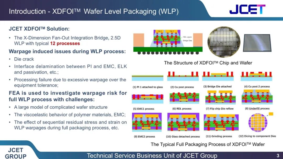
JCET XDFOITM Solution: The X-Dimension Fan-Out Integration Bridge, 2.5D WLP with complicated typical 12 processes as shown in Figure 1.
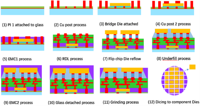
Figure 1. The typical full packaging process of XDFOITM wafer
Warpage induced issues during WLP process: Die crack; Interface delamination between PI and EMC, ELK and passivation, etc.; Processing failure due to excessive warpage over the equipment tolerance.
FEA is used to investigate warpage risk for full WLP process with challenges: A large model of complicated wafer structure; The viscoelastic behavior of polymer materials, EMC; The effect of sequential residual stress and strain on WLP warpages during full packaging process, etc.
使用工具
Equivalent calculation by energy approach and force, strain equivalent method to simplify the wafer mic-structure as shown in Figure 2.
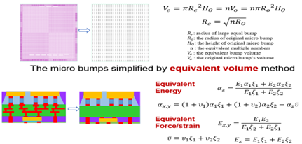
Figure 2. The equivalent calculation methods
Ansys Mechanical with element birth and death method to simulate the full packaging process as shown in Figure 3.
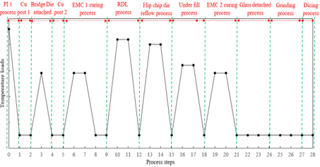
Figure 3. The thermal loads during WLP full packaging process with element birth & death method
最终成果
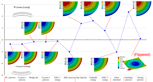
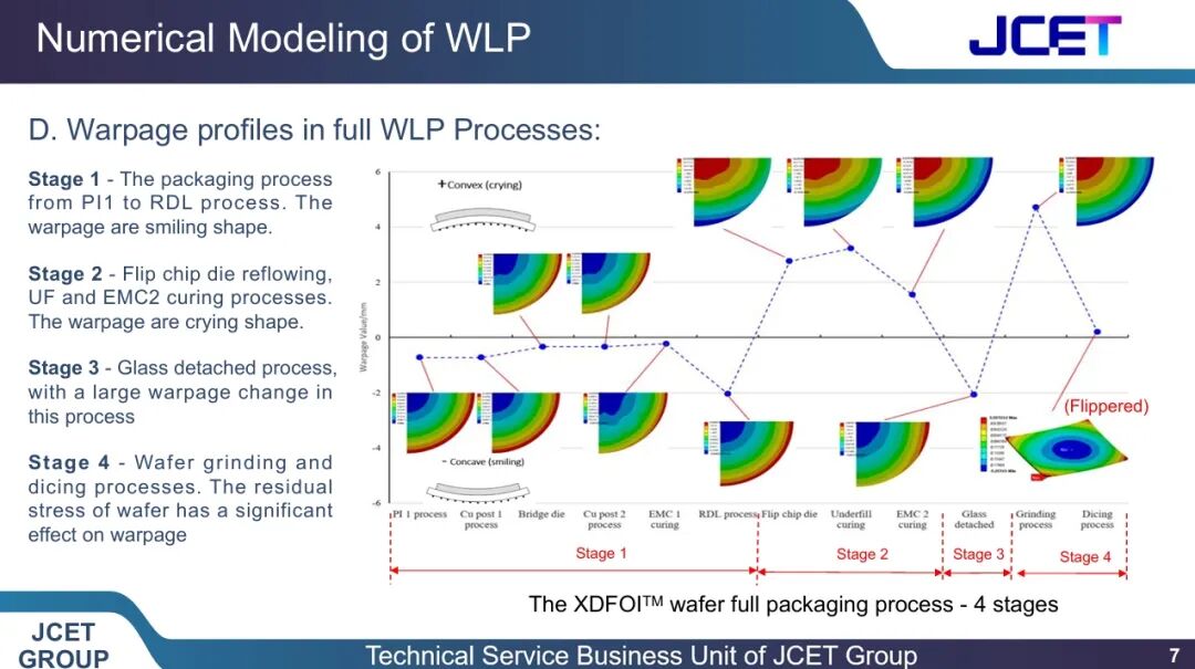
Figure 4. The XDFOITM wafer full packaging process
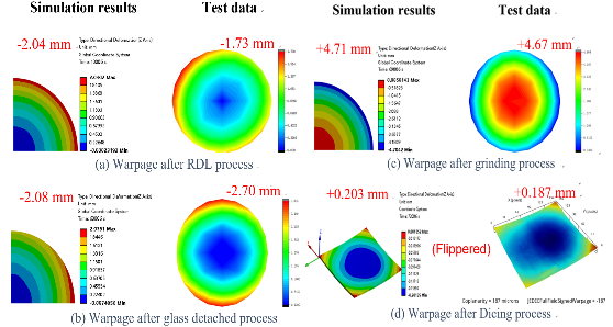
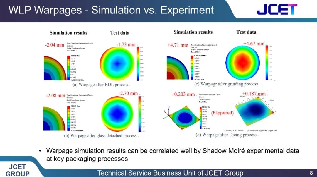
Figure 5. Simulation results validated by test data well
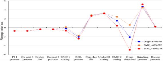
Figure 6. Warpages of XDFOITM during full packaging process with different CTEs of EMC
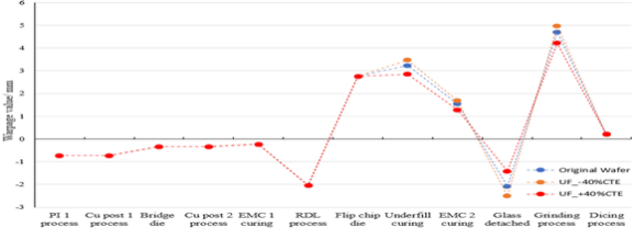
Figure 7. Warpages of XDFOITM wafer during full packaging process with different CTEs of UF
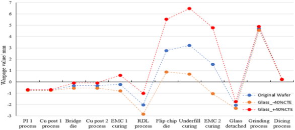
Figure 8. Warpages of XDFOITM wafer during full packaging process with different CTEs of glass
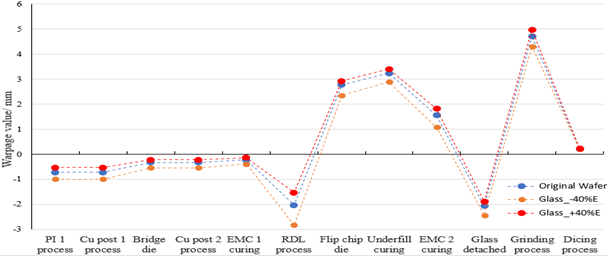
Figure 9.Warpages of XDFOITM wafer during full packaging process with different Young’s modules of glass
The full WLP processes of XDFOITM are introduced
Modeling approach with element birth and death method and structures equivalent are used to investigate the warpages of the XDFOITM
Numerical modeling warpages can be correlated well with test data
The effects of key parameters, ETC and Young’s Modulus on WLP wafer during full process are also studied in this paper
Reducing CTE of EMC would significantly reduce the warpages in glass detached process
Increasing the CTE of UF would reduce the WLP wafer warpage
Decreasing the CTE and Young’s modulus of glass would significantly decrease the warpage in stage 2, flip chip die, UF and EMC2 curing processes
参赛作品一览
左右滑动查看更多