
140GHz 毫米波大突破!5.2 米传 16Gbps,CMOS 工艺让 6G 通信更近了

而要实现这个目标,毫米波技术尤其是 110-170GHz 的 W 波段,早已被业界视为 6G 时代的 “核心赛道”。但高频段带来的空间损耗、高成本、覆盖窄等问题,一直是商业化的 “拦路虎”。
新书推荐:CMOS射频集成电路设计与仿真
今天看到《IEEE Transactions on Microwave Theory and Techniques》(微波领域顶刊)上面的一篇论文,直接给出了破局方案:一款基于 CMOS 工艺的 140GHz 8×8 收发相控阵系统,不仅实现了 5.2 米距离下 16Gbps 的高速传输,还兼具低成本、可扩展的优势,为毫米波通信的落地按下了 “加速键”。
高频段通信的三大 “老大难”
为什么 140GHz 这样的高频段这么香,却一直没普及?核心是三个绕不开的难题:
空间损耗惊人
140GHz 的信号衰减速度远快于我们熟悉的 5G Sub-6GHz 频段,就像声音在大风中传播一样,没走多远就变弱,需要更强的信号辐射和更高增益的天线才能 “传得远”; 系统成本居高不下
传统毫米波设备依赖 GaAs 等化合物半导体,不仅量产难度大,价格也昂贵,很难大规模应用在消费电子、物联网等场景; 覆盖范围太窄
高频信号方向性强,普通天线很难实现宽角度通信,无法满足 VR 设备移动、基站多用户覆盖等需求。
所以这篇论文的核心思路,就是用 “高集成 + CMOS 工艺”,一次性解决这三大痛点。
二、硬核设计:单芯片集成的 “信号集团军”
这篇论文的最大亮点,在于把复杂的毫米波系统 “浓缩” 到了一块芯片上,堪称通信硬件的 “集成化典范”。我们用通俗的语言拆解它的核心设计:
1. 核心架构:8×8 收发相控阵,像 “信号集团军” 协同作战
整个系统的核心是一块 8×8 通道的收发(TRX)相控阵芯片 —— 相当于 8×8=64 个 “迷你信号站” 协同工作。每个 “迷你信号站” 都有独立的发射 / 接收电路,还能通过 4 位相位和 4 位增益控制,精准调节自己的信号方向和强度。如下图所示
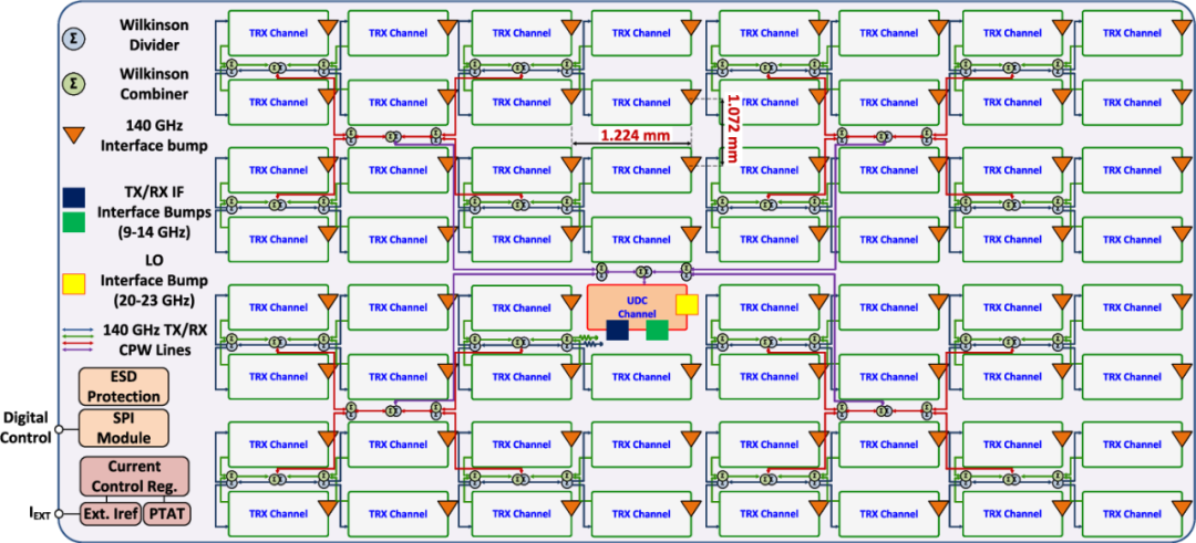
Fig. 1. Block diagram of 2-D 140-GHz 8 × 8 TRX array with UDC to IF.
这种设计的好处是:通过 64 个通道的 “波束成形”,能把分散的信号集中成一束强波束,既提升了信号辐射强度(对抗空间损耗),又能灵活调整波束方向,实现宽角度覆盖。
2. 关键组件:“信号翻译官”+“高效传输网”
上下变频器(UDC)
相当于 “信号翻译官”。它被集成在芯片上,负责把 PCB 板上的 9-14GHz 中频信号(IF),转换成 140GHz 的毫米波信号(RF),反之也能把接收的毫米波信号还原成中频信号。 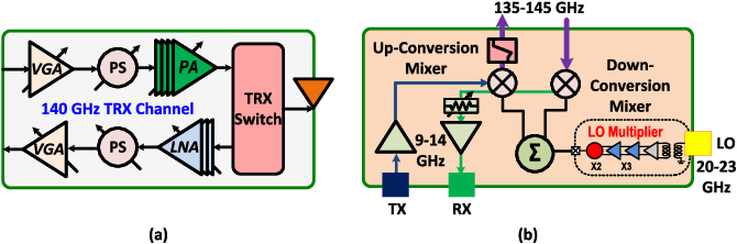
Fig. 2. Details of the (a) TRX, (b) UDC channels. 有了它,芯片就能和普通电路无缝对接,不用额外搭建复杂的频率转换模块; 射频分配网络(DN)
相当于 “高效传输网”。由共面波导、威尔金森分合路器、线路放大器组成,负责把信号均匀分配到 64 个通道,同时放大信号,避免传输过程中的损耗。
3. 工艺亮点:CMOS 加持,成本直接 “打下来”
芯片采用了 GlobalFoundries 的 45RFSOI CMOS 工艺 —— 这是消费电子领域主流的量产工艺(比如手机芯片常用 CMOS)。相比传统的 GaAs 工艺,CMOS 工艺不仅能实现更高的集成度,还能大幅降低量产成本,这意味着未来这款设备有望走进消费电子、物联网等大众场景。
4. 封装与天线:低成本也能有高性能
芯片被倒装在一块 “低成本有机 RF PCB” 上,PCB 上还集成了 8×8 的贴片天线阵列。天线的栅格设计得非常紧凑(1.07×1.22mm²),在 140GHz 频段下相当于信号波长的 0.5-0.57 倍,既能保证天线增益,又能控制整体尺寸,适配各类设备。
三、实测封神:5.2 米 16Gbps,性能拉满!
一款技术好不好,最终要看实测数据。这篇论文通过 “空中测试(OTA)”,交出了一份亮眼的成绩单:
1. 覆盖能力:宽角度扫描,告别 “信号死角”
水平面(H 面):支持 ±60° 扫描,垂直面(E 面):支持 ±38° 扫描; 不管是发射还是接收模式,都能实现这个覆盖范围 —— 意味着拿着 VR 设备移动、或者多个用户同时连接,都能稳定通信,不用再担心 “信号断联”。
2. 信号强度与接收性能:硬抗空间损耗
发射端(TX):在 137.5-145GHz 频段,峰值有效辐射功率(EIRP)达到 34-37.5dBm—— 相当于把 64 个 “迷你信号站” 的力量集中起来,足以对抗 140GHz 的强衰减; 接收端(RX):在 134-143GHz 频段,1dB 压缩点达到 - 12~-9dBm—— 说明接收灵敏度很高,即使是微弱的信号也能准确接收,还不会因为信号过强而失真。
3. 传输速度:16Gbps@5.2 米,满足超高清需求
这是最核心的实测数据,直接验证了系统的实用价值:
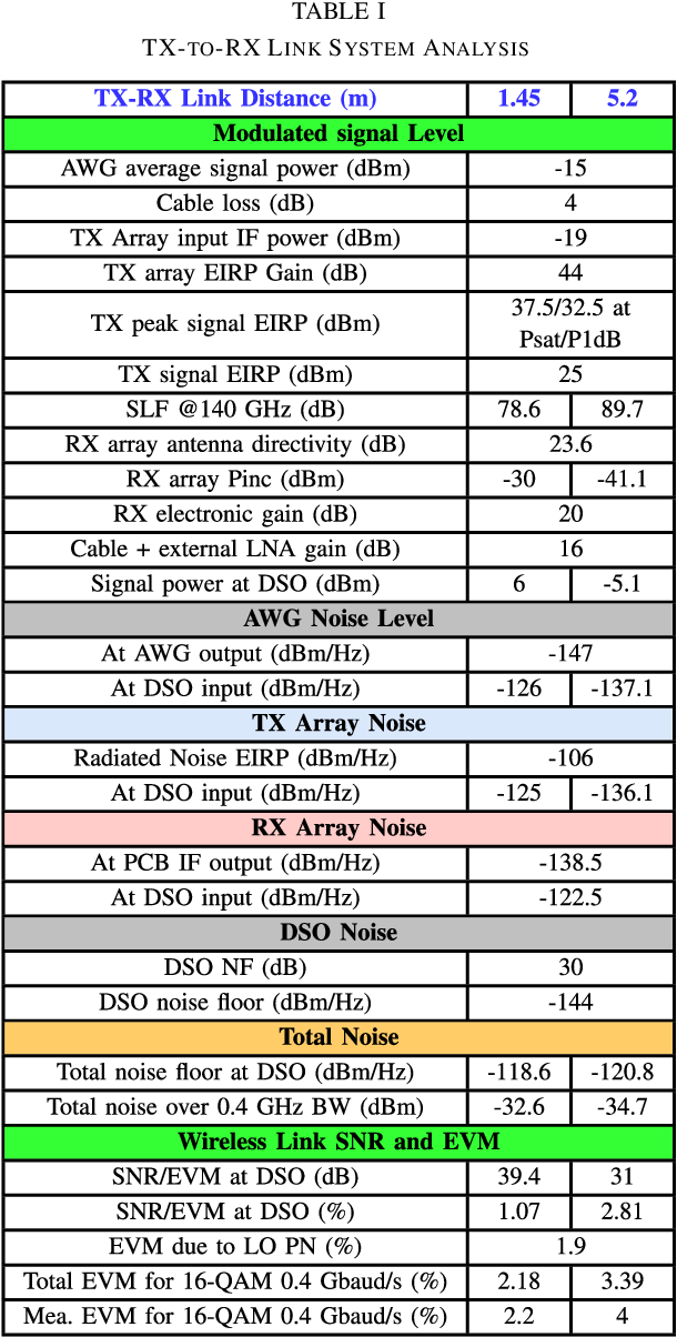
支持 16-QAM 和 64-QAM 两种高阶调制方式(调制方式越高级,频谱效率越高,传输速度越快); 极限速度:最高能达到 24Gbps(64-QAM 调制),信号质量误差(rms EVM)小于 6%—— 这个速度足以传输 8K 超高清视频,延迟还能控制在微秒级; 远距离实测: 1.45 米距离:20Gbps(16-QAM),信号质量误差小于 9%; 5.2 米距离:16Gbps(16-QAM),信号质量误差小于 9%。
要知道,这是 140GHz 频段少有的 “5 米级 + 10Gbps+” 实测结果,直接打破了高频段 “只能短距离传输” 的刻板印象。
四、应用前景:从 VR/AR 到 6G,覆盖多场景
这款技术的落地,将直接推动多个领域的升级:
VR/AR 设备
:16-24Gbps 的高速传输 + 微秒级低延迟,能实现超高清画面的无线传输,摆脱 VR 设备的有线束缚,让沉浸式体验更自然; 高速无线回程
:基站与基站、数据中心与数据中心之间,不用再铺设有线光纤,用这款设备就能实现点对点的高速连接,降低部署成本和维护难度; 物联网(IoT)
:6G 时代将有海量设备联网,140GHz 的宽频谱能支持更多设备同时连接,还能满足工业设备、智能终端的高速数据传输需求; 短距离高速传输
:比如服务器机房、工业车间里的设备间数据交互,用无线替代有线,提升设备布局的灵活性。
五、总结:毫米波通信的 “平民化” 曙光
这篇论文的核心贡献,不仅是实现了 “5.2 米 16Gbps” 的性能突破,更重要的是验证了 “CMOS 工艺 + 高集成相控阵” 的可行性 —— 它让毫米波设备从 “昂贵的实验室产物”,变成了 “可量产、低成本的商用产品”。
随着 6G 技术的推进,140GHz 这样的高频段将成为核心通信频段。而这篇论文提出的设计思路,为后续更大规模、更远距离、更高速度的毫米波系统提供了重要参考。或许用不了多久,我们就能在 VR 设备、智能汽车、工业物联网中,感受到这项技术带来的高速与便捷。
你觉得 6G 时代,毫米波还会有哪些惊喜应用?欢迎在评论区留言讨论~
论文来源:IEEE Transactions on Microwave Theory and Techniques(2024 年 5 月)论文 DOI:10.1109/TMTT.2023.3346
论文标题:140-GHz 2-D Scalable On-Grid 8⨉ 8-Element Trans mit–Receive Phased Arrays With Up/Down Converters Demonstrating a 5.2-m Link at 16 Gbps | IEEE Journals & Magazine | IEEE Xplore
如果有同学可以下载原文的话,可以在评论区分享一下。
论文图示:
Fig. 1. Block diagram of 2-D 140-GHz 8 × 8 TRX array with UDC to IF.
Fig. 2. Details of the (a) TRX, (b) UDC channels.
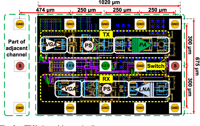
Fig. 3. TRX channel layout details.
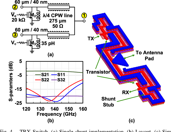
Fig. 4. TRX Switch. (a) Single-shunt implementation. (b) Layout. (c) Simulation results.
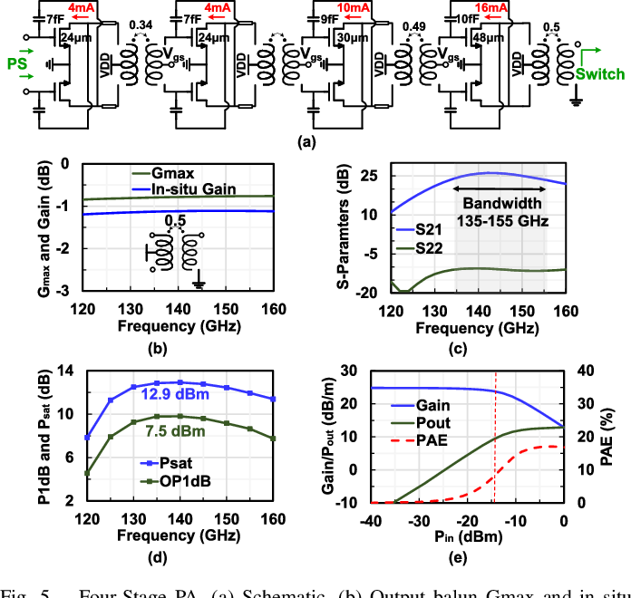
Fig. 5. Four-Stage PA. (a) Schematic. (b) Output balun Gmax and in situ gain. (c) Gain and output matching. (d) Output P1dB and Psat. (e) PAE, gain, and Pout versus input power.
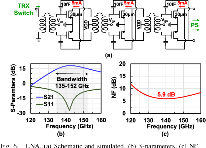
Fig. 6. LNA. (a) Schematic and simulated. (b) S-parameters. (c) NF.
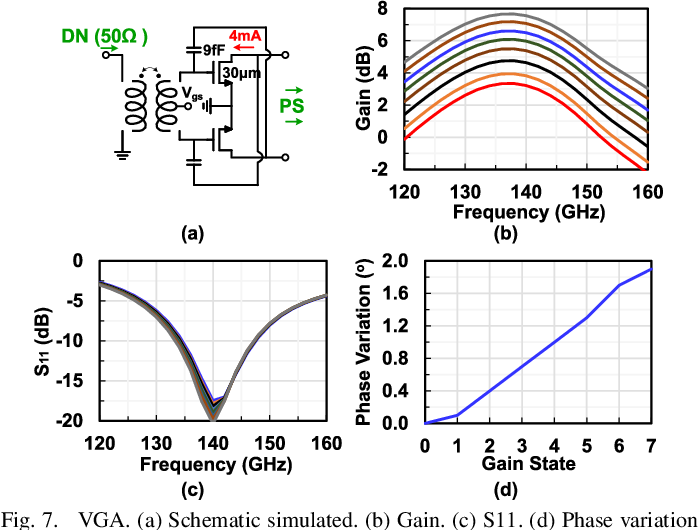
Fig. 7. VGA. (a) Schematic simulated. (b) Gain. (c) S11. (d) Phase variation across gain states.
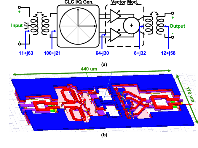
Fig. 8. PS. (a) Block diagram. (b) Full EM layout.
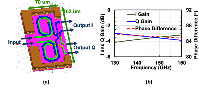
Fig. 9. CLC. (a) EM structure. (b) Simulated results.
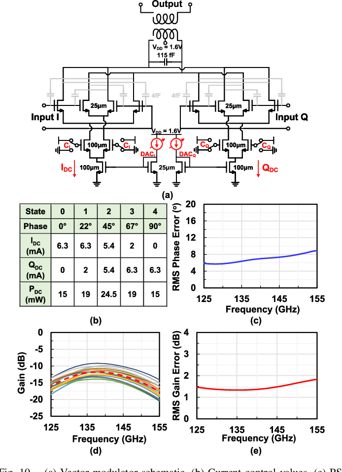
Fig. 10. (a) Vector modulator schematic. (b) Current control values. (c) PS rms phase error. (d) Gain for all phase states. (e) rms gain error.
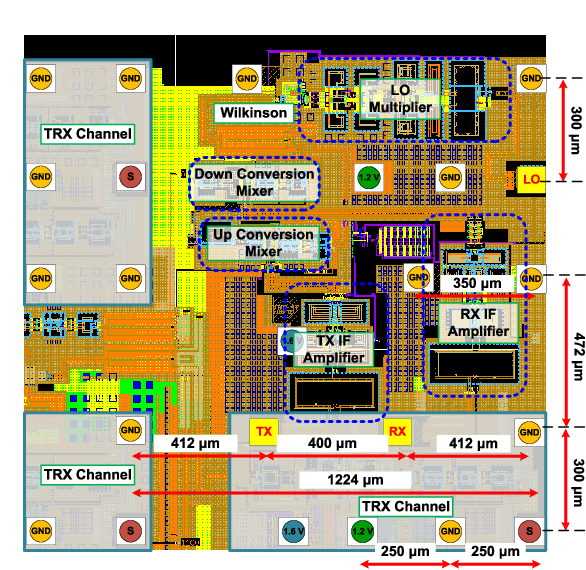
Fig. 11. UDC channel layout details.
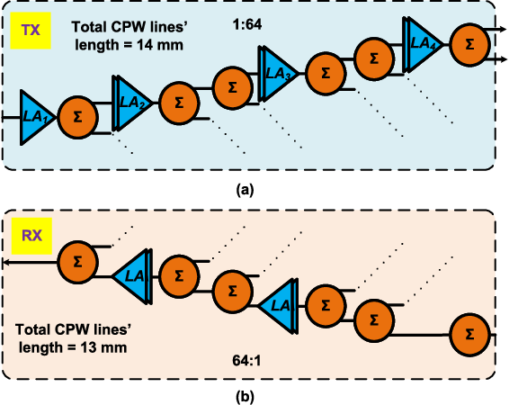
Fig. 12. DN block diagram for (a) TX and (b) RX.
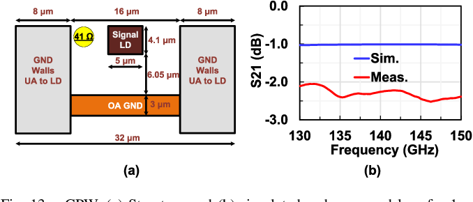
Fig. 13. CPW. (a) Structure and (b) simulated and measured loss for 1-mm line.
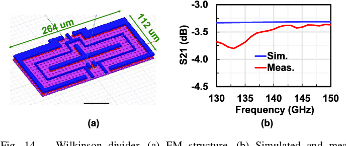
Fig. 14. Wilkinson divider. (a) EM structure. (b) Simulated and measured S21.
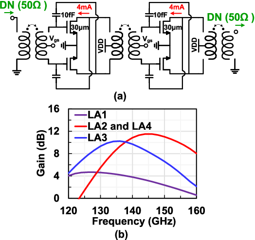
Fig. 15. Line amplifier. (a) Schematic. (b) Simulated gain.
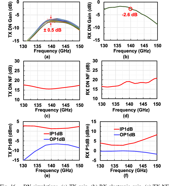
Fig. 16. DN simulations. (a) TX gain. (b) RX electronic gain. (c) TX NF. (d) RX NF. (e) TX P1dB. (f) RX P1dB.
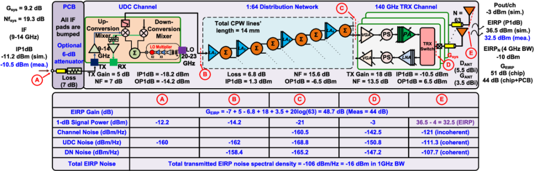
Fig. 17. System-level calculation for the 8 × 8 TRX array (TX operation).
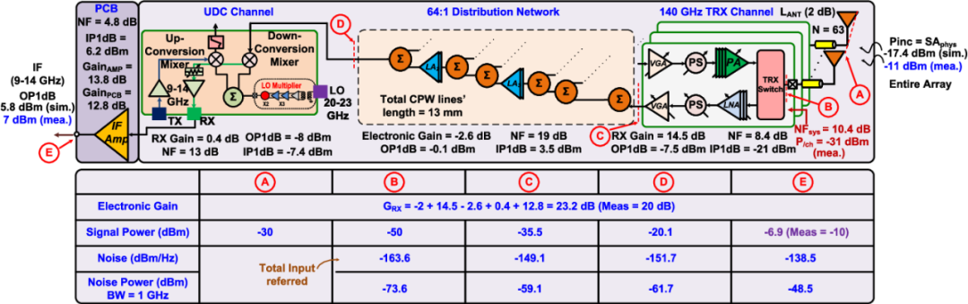
Fig. 18. System-level calculation for the 8 × 8 TRX array (RX operation).
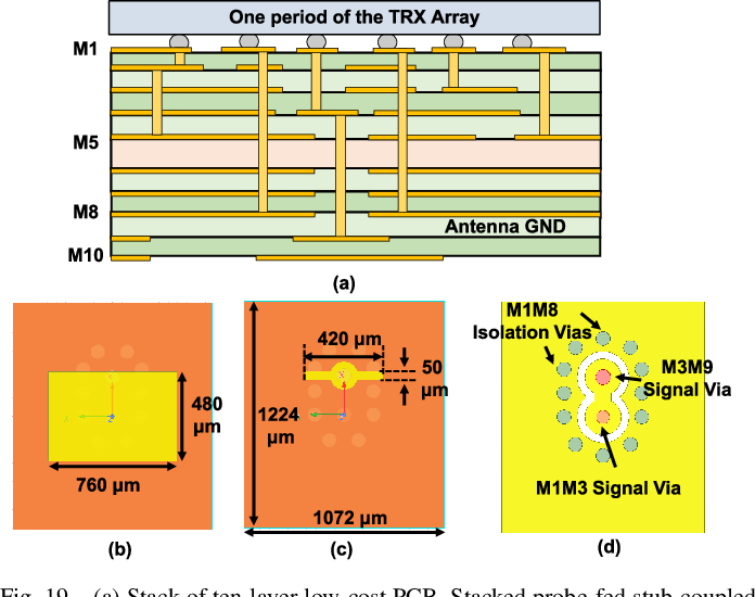
Fig. 19. (a) Stack of ten-layer low-cost PCB. Stacked probe-fed stub-coupled microstrip antenna details of (b) M10 patch, (c) M9 stub, and (d) transition on M3.
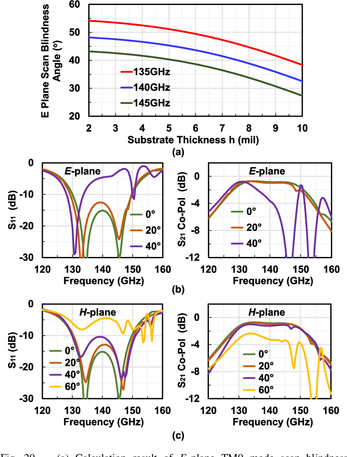
Fig. 20. (a) Calculation result of E-plane TM0 mode scan blindness angle versus different substrate thickness. HFSS simulated S11 and co-pol result under different scanning conditions in co-design model, including chip, bumps, and antenna for (b) E-plane and (c) H -plane
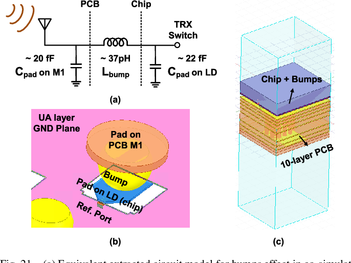
Fig. 21. (a) Equivalent extracted circuit model for bumps effect in co-simulate model. (b) Detailed view of reference port in chip-bump-antenna co-simulate model. (c) Ansys HFSS co-simulation model.
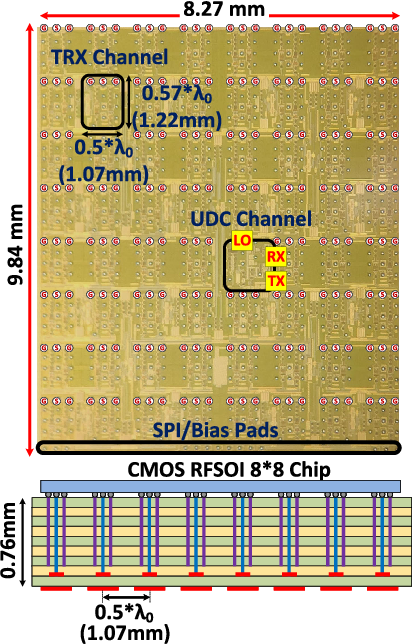
Fig. 22. Chip die photograph and cross section of the RF board.
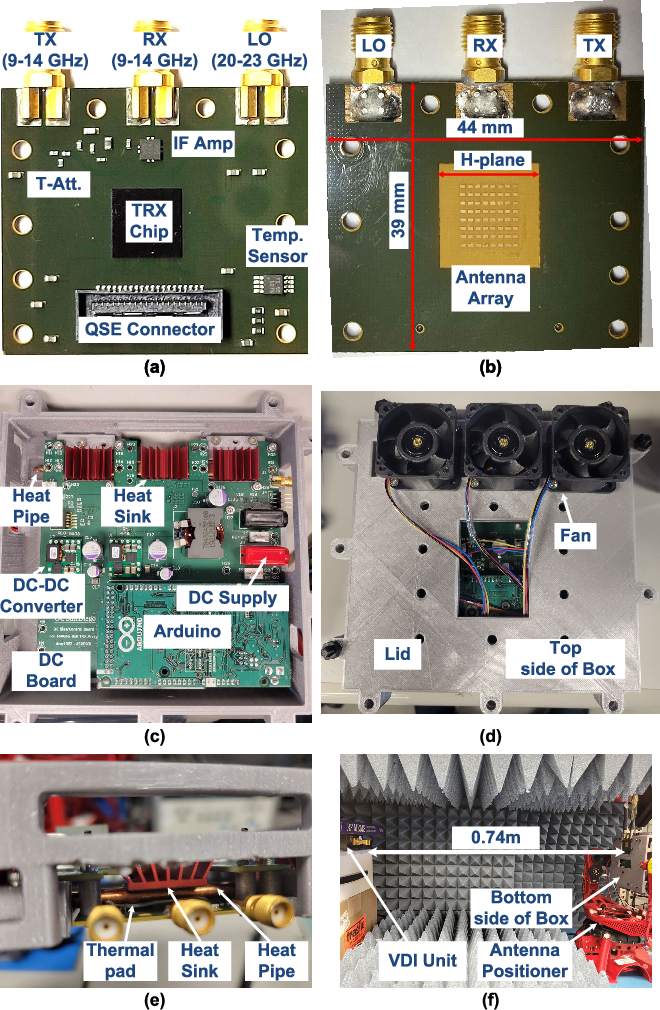
Fig. 23. (a) Top side of the RF PCB. (b) Bottom side showing the antenna array. (c) Top side of the DC board and the box. (d) Top side of the box with the lid on. (e) Side view looking into the RF board showing the thermal pad, heat pipe, and heat sink. (f) Bottom side of the box and the OTA measurement setup.
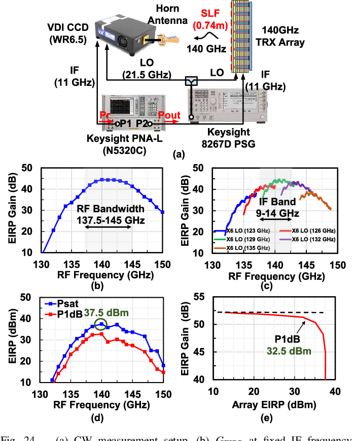
Fig. 24. (a) CW measurement setup. (b) GEIRP at fixed IF frequency. (c) GEIRP at swept IF frequency and different LO frequencies. (d) EIRP at saturation and at P1dB. (e) Array AM–AM response.
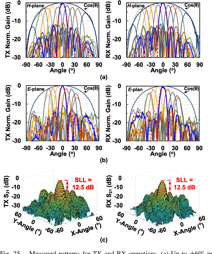
Fig. 25. Measured patterns for TX and RX operations. (a) Up to ±60◦ in the H -plane. (b) Up to ±38◦ in the E-plane. (c) Three-dimensional patterns at broadside with SLL better than 12.5 dB.
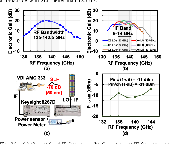
Fig. 26. (a) GRX at fixed IF frequency. (b) GRX at swept IF frequency and different LO frequencies. (c) Pinc-1-dB measurement setup. (d) Measured RX operation Pinc-1 dB.
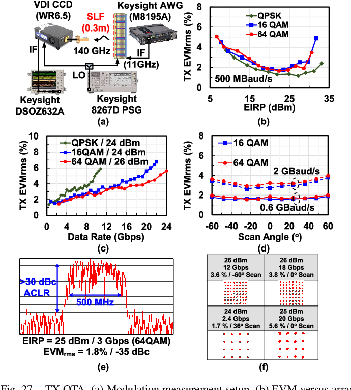
Fig. 27. TX OTA. (a) Modulation measurement setup. (b) EVM versus array EIRP at an example BW of 500 MHz. (c) EVM versus data rate. (d) EVM versus beam scan angle. (e) Array output spectrum (after DC with CCD unit). (f) Output constellation for different EIRP values, scan angles, and modulation types.
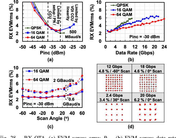
Fig. 28. RX OTA. (a) EVM versus array Pinc. (b) EVM versus data rate. (c) EVM versus beam scan angle. (d) Output constellation at different scan angles and modulation types (Pinc = −30 dBm).
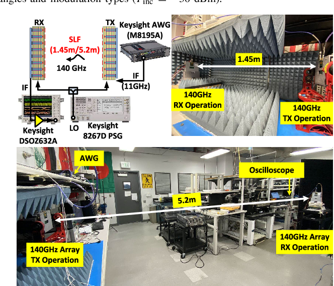
Fig. 29. TX–RX communication link measurement setups.
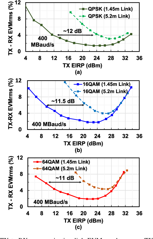
Fig. 30. TX-to-RX communication link EVM results versus TX EIRP for (a) QPSK, (b) 16-QAM, and (c) 64-QAM signals.
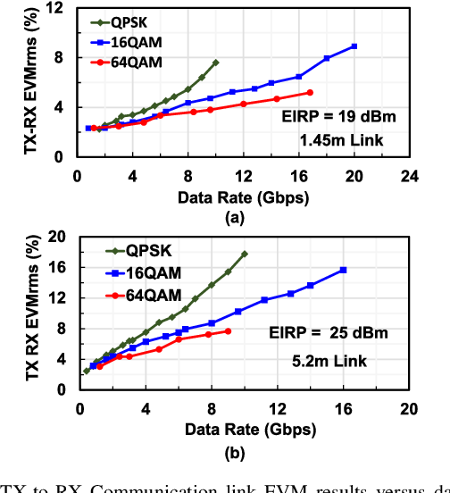
Fig. 31. TX-to-RX Communication link EVM results versus data rate for (a) 1.45-m link with 19-dBm EIRP and (b) 5.2-m link and 26-dBm EIRP.
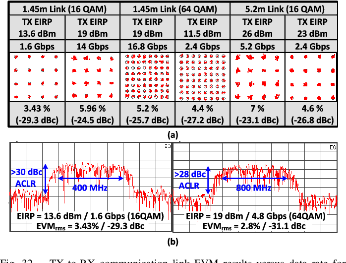
Fig. 32. TX-to-RX communication link EVM results versus data rate for (a) 1.45-m link with 19-dBm EIRP and (b) 5.2-m link and 26-dBm EIRP.

版权声明:射频学堂原创或者转载的内容,其版权皆归原作者所有,其观点仅代表作者个人,射频学堂仅用于知识分享。如需转载或者引用,请与原作者联系。射频学堂转述网络文章,皆著名来源和作者,不可溯源文章除外,如有异议,请与我们联系。