DDR4 SDRAM - Understanding Timing Parameters

Introduction
There are a large number oftiming parameters in the DDR standard, but when you work with DDR4 SDRAM you'lloften find yourself revisiting or reading about a handful of timing parametersmore often than others. So, in this article we'll examine only these frequentlyoccurring timing parameters by looking at them in the context of a command.
These timing parameters are a hard thing to remember, they tend to slip out of your head. The accompanying article, Timing Parameter Cheat Sheet, can be used as a reference to recollect what a specific timing parameter means.
Note: All pictures below were taken from the DDR4 JEDEC specification and a Micron memory part spec. Links to them can be found in the Reference section.
ACTIVATE Timing
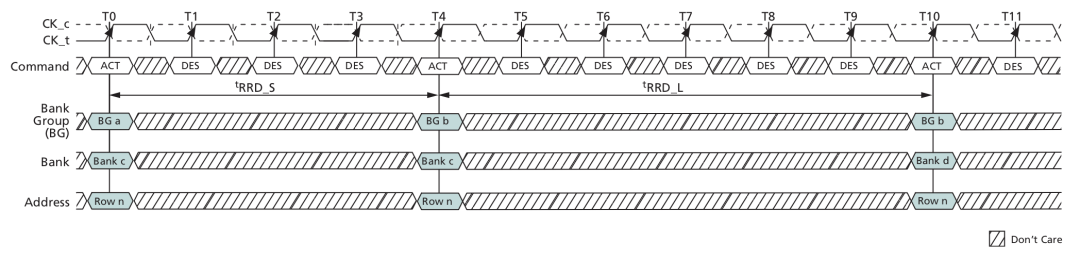
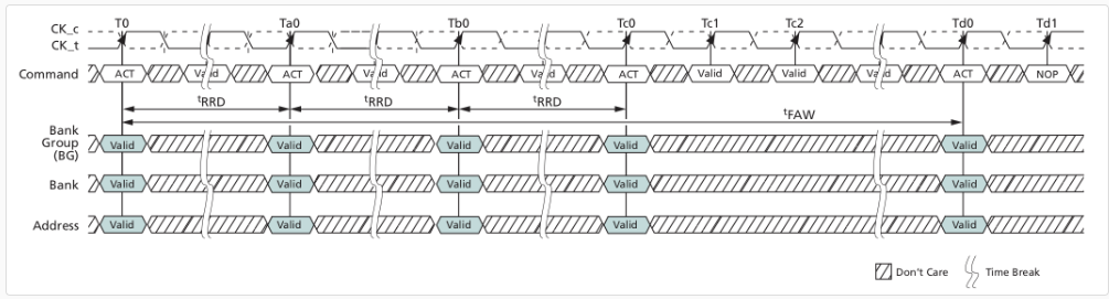
The ACTIVATE command is used to open a row within a bank. In Understanding the Basics we saw that every bank has a set of sense amps, so one row can remain active per bank. With ACTIVATE there are 3 timing parameters we should know about: tRRD_S, tRRD_L, tFAW

Table 1: Activate command timing parameters
REFRESH Timing
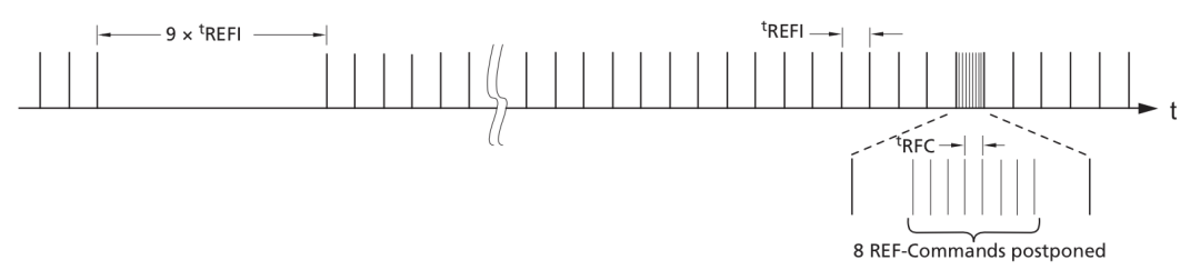
In order to ensure data stored in the SDRAM is not lost, the memory controller has to issue a REFRESH command at an average interval of tREFI. But before a REFRESH can be applied, all banks of the SDRAM have to be Precharged and idle for a minimum time of tRP(min). Once a REFRESH command is issued, there has to be a delay of tRFC(min) before the next valid command is issued (except DES command).
Notice how I mentioned that tREFI is the "average" interval between REFRESH commands. This is because you can push-out (or pull-in) a certain number of refresh commands and make up for it later. This mode was added to DDR4 to overcome the performance penalty due to refresh lockout at the higher densities. The number of refresh commands that can be postponed depends upon the Refresh Mode (1x, 2x or 4x) which can be set in the SDRAM's Mode Register MR2.


READ Timing
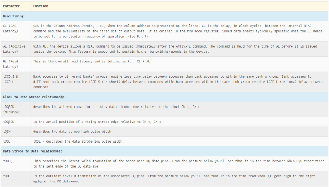
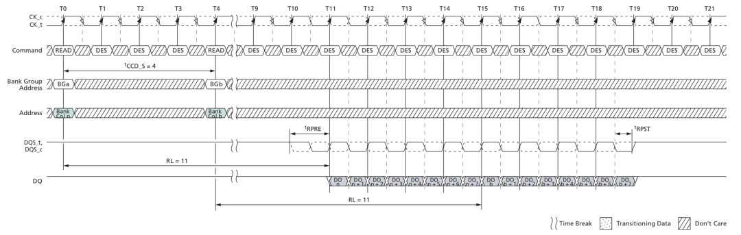
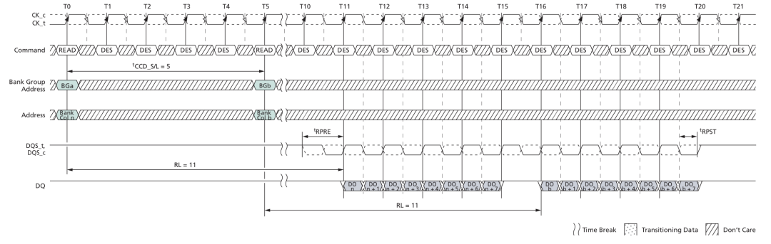
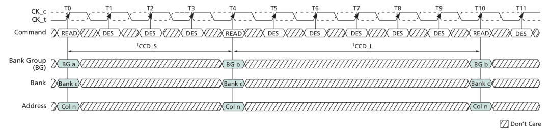
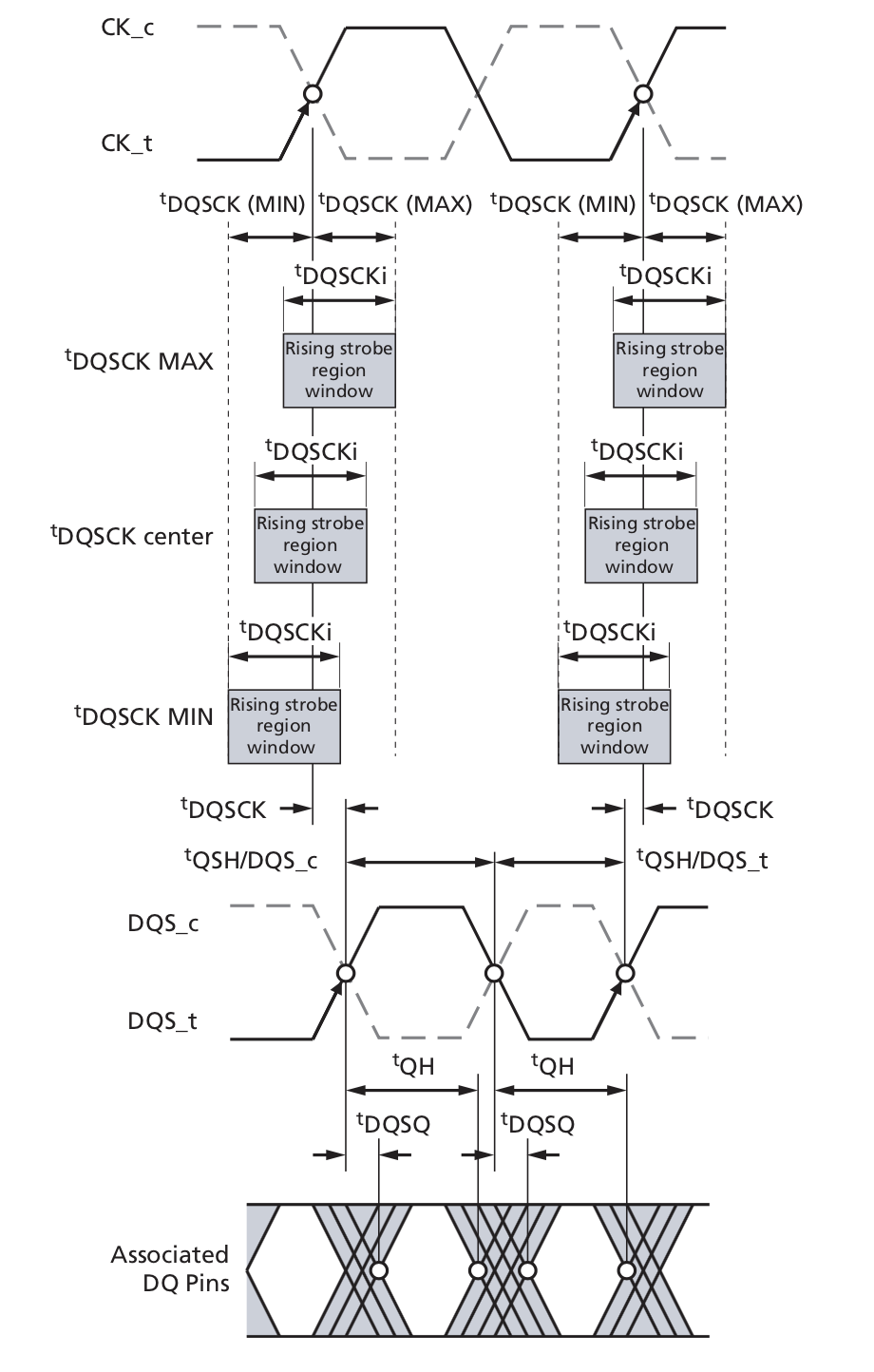
The READ timing parameters can be broken up into 3 categories - Overall read timing, Clock-to-Strobe relationship and Data Strobe-to-Data relationship. Refer to DRAM-read-operation to understand the basics.
WRITE Timing
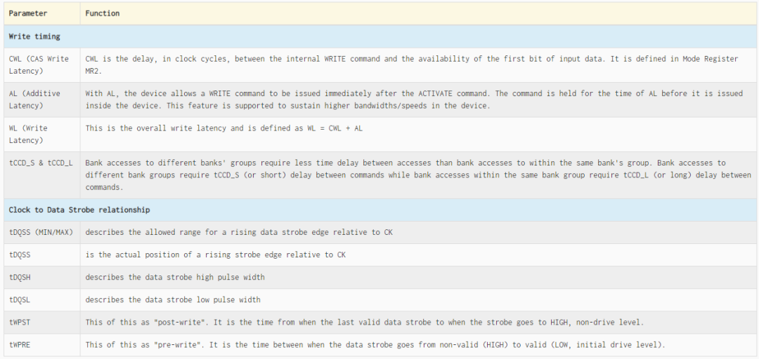
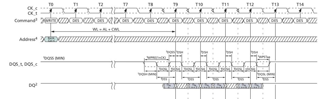
Following similarly to the READ ...
Mode Register Timing
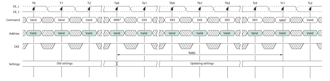
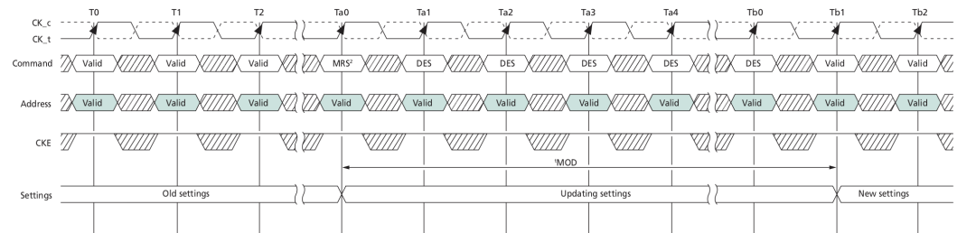
SDRAMs provide a number of features, functions and settings which can be programmed using the 7 Mode Registers. These registers can be programmed using the MRS (Mode Register Set) command. The Mode Registers are set during initialization and thereafter they can be changed at any time during normal operation. Mode Register setting is governed by two timing parameters.