混合信号与数字信号处理设计技术AD转换时的信噪比分析的很精彩-电子书400页

混合信号与数字信号处理设计技术(Mixed-Signal and DSP Design Techniques) AD转换时的信噪比分析的很精彩
摘要:
《DSP 算法综合与优化》聚焦数字信号处理算法的硬件化实现与自动化优化,围绕多字长定点设计展开系统研究。书中提出信号峰值估计、字长优化与饱和运算分析方法,建立解析噪声模型与面积代价模型,兼顾线性与非线性系统。通过启发式搜索与混合整数线性规划实现字长最优分配,结合调度与资源绑定完成多字长架构综合。全书覆盖 FPGA/ASIC 实现、自适应滤波、滤波器设计等典型场景,可在满足精度约束下最小化面积、降低功耗并提升运行速度,为 DSP 算法高效硬件实现提供完整理论与工程方法。
SECTION 1 INTRODUCTION
Walt Kester
ORIGINS OF REAL-WORLD SIGNALS AND THEIR UNITS OF MEASUREMENT
In this book, we will primarily be dealing with the processing of real-world signals using both a nalog and digital techniques. Before starting, however, let's look at a
few key concepts and definitions required to lay the groundwork for things to come.
Webster's New Collegiate Dictionary defines a signal as "A detectable (or
measurable) physical quantity or impulse (as voltage, current, or magnetic field strength) by which messages or information can be trans mitted." Key to this
definition are the words: detectable, physical quantity, and information.
SIGNAL CHARACTERISTICS
■ Signal Characteristics
◆ Signals are Physical Quantities
◆ Signals are Measurable
◆ Signals Contain Information
◆ All Signals are A nalog
■ Units of Measurement
◆ Temperature: °C
◆ Pressure: Newtons/m2
◆ Mass: kg
◆ Voltage: Volts
◆ Current: Amps
◆ Power: Watts
Figure 1.1
By their very nature, signals are an alog , whether DC, AC, digital levels, or pulses. It is customary, however, to differentiate between a nalog and digital signals in the following manner: An alog (or real.world) variables in nature include all measurable physical quantities. In this book, an alog signals are generally limited to electrical variables, their rates of change, and their associated energy or power levels. Sensors are used to convert other physical quantities (temperature, pressure, etc.) to electrical signals. The entire subject of signal conditioning deals with preparingreal.world signals for processing and includes such topics as sensors (temperature and pressure, for example), isolation and instrumentation amplifiers, etc. (see Reference 1).
Some signals result in response to other signals. A good example is the returned signal from a radar or ultrasound imaging system, both of which result from a known trans mitted signal.
On the other hand, there is another classification of signals, called digital, where the actual signal has been conditioned and formatted into a digit. These digital signals may or may not be related to real.world a nalog variables. Examples include the data trans mitted over local area networks (LANs) or other high speed networks.
In the specific case of Digital Signal Processing (DSP), the an alog signal is converted into binary form by a device known as an an alog.to.digital converter (ADC). The output of the ADC is a binary representation of the an alog signal and is manipulated arithmetically by the Digital Signal Processor. After processing, the information obtained from the signal may be converted back into an alog form using a digital.to.an alog converter (DAC).
Another key concept embodied in the definition of signal is that there is some kind of information contained in the signal. This leads us to the key reason for processing real.world an alog signals: the extraction of information.
REASONS FOR PROCESSING REAL-WORLD SIGNALS
The primary reason for processing real.world signals is to extract information from them. This information normally exists in the form of signal amplitude (absolute or relative), frequency or spectral content, phase, or timing relationships with respect to other signals. Once the desired information is extracted from the signal, it may be used in a number of ways.
In some cases, it may be desirable to reformat the information contained in a signal. This would be the case in the trans mission of a voice signal over a frequency division multiple access (FDMA) telephone system. In this case, an alog techniques are used to "stack" voice channels in the frequency spectrum for trans mission via microwave relay, coaxial cable, or fiber. In the case of a digital trans mission link,
the an alog voice information is first converted into digital using an ADC. The digital information representing the individual voice channels is multiplexed in time (time division multiple access, or TDMA) and trans mitted over a serial digital trans mission link (as in the T.Carrier system).
Another requirement for signal processing is to compress the frequency content of the signal (without losing significant information) then format and trans mit the information at lower data rates, thereby achieving a reduction in required channel bandwidth. High speed modems and adaptive pulse code modulation systems (ADPCM) make extensive use of data reduction algorithms, as do digital mobile radio systems, MPEG recording and playback, and High Definition Television (HDTV).
Industrial data acquisition and control systems make use of information extracted from sensors to develop appropriate feedback signals which in turn control the process itself. Note that these systems require both ADCs and DACs as well as sensors, signal conditioners, and the DSP (or microcontroller). An alog Devices offers a family of MicroConverters™ which include precision an alog conditioning circuitry, ADCs, DACs, microcontroller, and FLASH memory all on a single chip.
In some cases, the signal containing the information is buried in noise, and the primary objective is signal recovery. Techniques such as filtering, auto.correlation, convolution, etc. are often used to accomplish this task in both the an alog and digital domains.
REASONS FOR SIGNAL PROCESSING
■ Extract Information About The Signal (Amplitude, Phase, Frequency, Spectral Content, Timing Relationships)
■ Reformat the Signal (FDMA, TDMA, CDMA Telephony)
■ Compress Data (Modems, Cellular Telephone, HDTV, MPEG)
■ Generate Feedback Control Signal (Industrial Process Control)
■ Extract Signal From Noise (Filtering, Autocorrelation, Convolution)
■ Capture and Store Signal in Digital Format for An alysis (FFT Techniques)
GENERATION OF REAL-WORLD SIGNALS
In most of the above examples (the ones requiring DSP techniques), both ADCs and DACs are required. In some cases, however, only DACs are required where real.
world an alog signals may be generated directly using DSP and DACs. Video raster scan display systems are a good example. The digitally generated signal drives a video or RAMDAC. Another example is artificially synthesized music and speech.
In reality, however, the real.world an alog signals generated using purely digital techniques do rely on information previously derived from the real.world equivalent an alog signals. In display systems, the data from the display must convey the appropriate information to the operator. In synthesized audio systems, the
statistical properties of the sounds being generated have been previously derived using extensive DSP a nalysis (i.e.,sound source, microphone, preamp, ADC, etc.).
METHODS AND TECHNOLOGIES AVAILABLE FOR PROCESSING REAL-WORLD SIGNALS
Signals may be processed using a nalog techniques (an alog signal processing, or ASP), digital techniques (digital signal processing, or DSP), or a combination of a nalog and digital techniques (mixed signal processing, or MSP). In some cases, the choice of techniques is clear; in others, there is no clear cut choice, and second.order considerations may be used to make the final decision.
With respect to DSP, the factor that distinguishes it from traditional computer a nalysis of data is its speed and efficiency in performing sophisticated digital processing functions such as filtering, FFT an alysis, and data compression in real time.
The term mixed signal processing implies that both an alog and digital processing is done as part of the system. The system may be implemented in the form of a printed circuit board, hybrid microcircuit, or a single integrated circuit chip. In the context of this broad definition, ADCs and DACs are considered to be mixed signal processors, since both a nalog and digital functions are implemented in each. Recent advances in Very Large Scale Integration (VLSI) processing technology allow complex digital processing as well as an alog processing to be performed on the same chip. The very nature of DSP itself implies that these functions can be performed in real-time.
AN ALOG VERSUS DIGITAL SIGNAL PROCESSING
Today's engineer faces a challenge in selecting the proper mix of an alog and digital techniques to solve the signal processing task at hand. It is impossible to process real.world an alog signals using purely digital techniques, since all sensors (microphones, thermocouples, strain gages, microphones, piezoelectric crystals, disk drive heads, etc.) are an alog sensors. Therefore, some sort of signal conditioning circuitry is required in order to prepare the sensor output for further signal processing, whether it be an alog or digital. Signal conditioning circuits are, in reality, an alog signal processors, performing such functions as multiplication (gain), isolation (instrumentation amplifiers and isolation amplifiers), detection in the presence of noise (high common.mode instrumentation amplifiers, line drivers, and line receivers), dynamic range compression (log amps, LOGDACs, and programmable gain amplifiers), and filtering (both passive and active).
Several methods of accomplishing signal processing are shown in Figure 1.3. The top portion of the figure shows the purely an alog approach. The latter parts of the figure show the DSP approach. Note that once the decision has been made to use DSP techniques, the next decision must be where to place the ADC in the signal path.
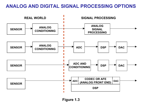
In general, as the ADC is moved closer to the actual sensor, more of the an alog signal conditioning burden is now placed on the ADC. The added ADC complexity may take the form of increased sampling rate, wider dynamic range, higher resolution, input noise rejection, input filtering and programmable gain amplifiers (PGAs), on.chip voltage references, etc., all of which add functionality and simplify the system. With today’s high.resolution/high sampling rate data converter technology, significant progress has been made in integrating more and more of the conditioning circuitry within the ADC/DAC itself. In the measurement area, for instance, 24.bit ADCs are available with built.in programmable gain amplifiers (PGAs) which allow fullscale bridge signals of 10mV to be digitized directly with no further conditioning (e.g. AD773x.series). At voiceband and audio frequencies, complete coder.decoders (Codecs – or An alog Front Ends) are available which have sufficient on.chip an alog circuitry to minimize the requirements for external conditioning components (AD1819B and AD73322). At video speeds, an alog front ends are also available for such applications as CCD image processing and others (e.g., AD9814, AD9816, and the AD984x series).
A PRACTICAL EXAMPLE
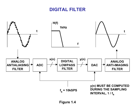
As a practical example of the power of DSP, consider the comparison between an an alog and a digital lowpass filter, each with a cutoff frequency of 1kHz. The digital filter is implemented in a typical sampled data system shown in Figure 1.4. Note that there are several implicit requirements in the diagram. First, it is assumed that an ADC/DAC combination is available with sufficient sampling frequency,
resolution, and dynamic range to accurately process the signal. Second, the DSP must be fast enough to complete all its calculations within the sampling interval, 1/fs. Third, a nalog filters are still required at the ADC input and DAC output for antialiasing and anti.imaging, but the performance demands are not as great.
Assuming these conditions have been met, the following offers a comparison between the digital and an alog filters.
The required cutoff frequency of both filters is 1kHz. The an alog filter is realized as a 6.pole Chebyshev Type 1 filter (ripple in pass band, no ripple in stopband), and the response is shown in Figure 1.5. In practice, this filter would probably be realized using three 2.pole stages, each of which requires an op amp, and several resistors and capacitors. Modern filter design CAD packages make the 6.pole design relatively straightforward, but maintaining the 0.5dB ripple specification requires accurate component selection and matching.
On the other hand, the 129.tap digital FIR filter shown has only 0.002dB pass band ripple, linear phase, and a much sharper roll off. In fact, it could not be realized using an alog techniques! Another obvious advantage is that the digital filter requires no component matching, and it is not sensitive to drift since the clock frequencies are crystal controlled. The 129.tap filter requires 129 multiply.
accumulates (MAC) in order to compute an output sample. This processing must be completed within the sampling interval, 1/fs, in order to maintain real.time operation. In this example, the sampling frequency is 10kSPS, therefore 100µs is available for processing, assuming no significant additional overhead requirement. The ADSP.21xx.family of DSPs can complete the entire multiply.accumulate process (and other functions necessary for the filter) in a single instruction cycle.
Therefore, a 129.tap filter requires that the instruction rate be greater than 129/100µs = 1.3 million instructions per second (MIPS). DSPs are available with instruction rates much greater than this, so the DSP certainly is not the limiting factor in this application. The ADSP.218x 16.bit fixed point series offers instruction rates up to 75MIPS.
The assembly language code to implement the filter on the ADSP.21xx.family of DSPs is shown in Figure 1.6. Note that the actual lines of operating code have been marked with arrows; the rest are comments.
更多内容见附件
免责声明:
本页面/内容部分素材来源于互联网公 开 信 息,旨在传递更多信息,不代表本平台立场。
版权归原作者或机构所有,如涉及侵权,请通过平台联系我们,我们将在核实后第一时间处理。
本平台对转载内容的真实性、准确性不作任何保证,用户需自行判断并承担使用风险