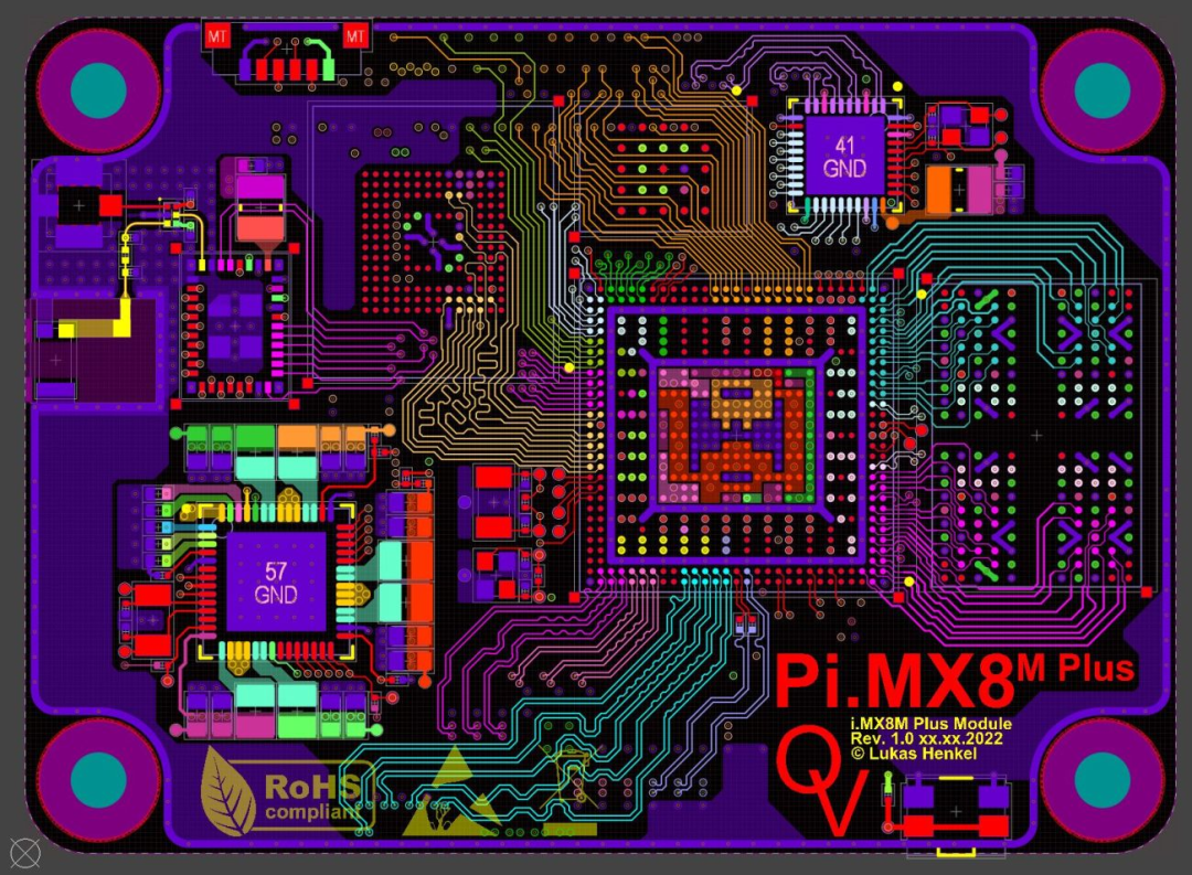
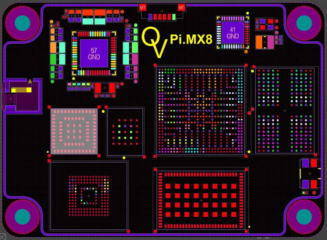
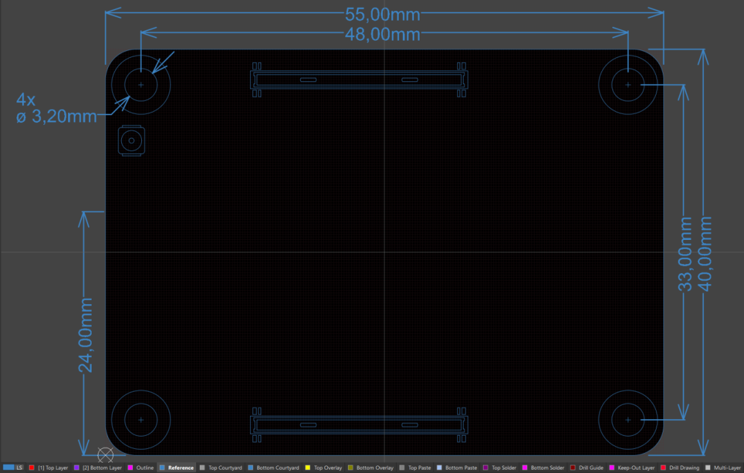
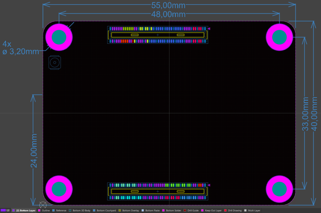
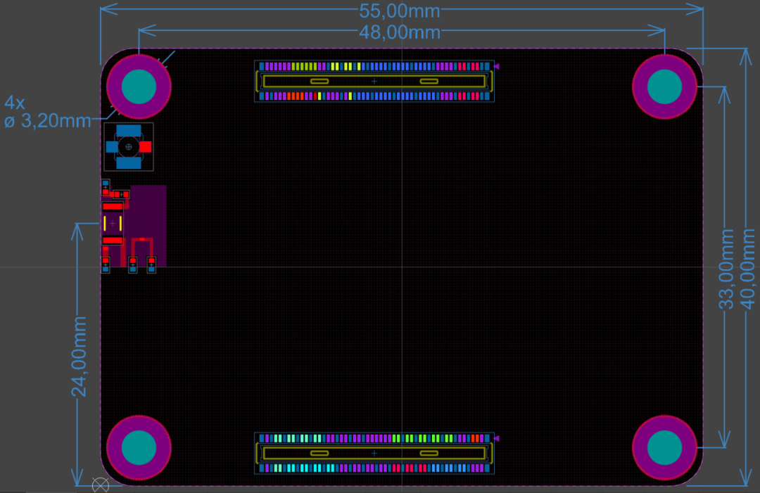
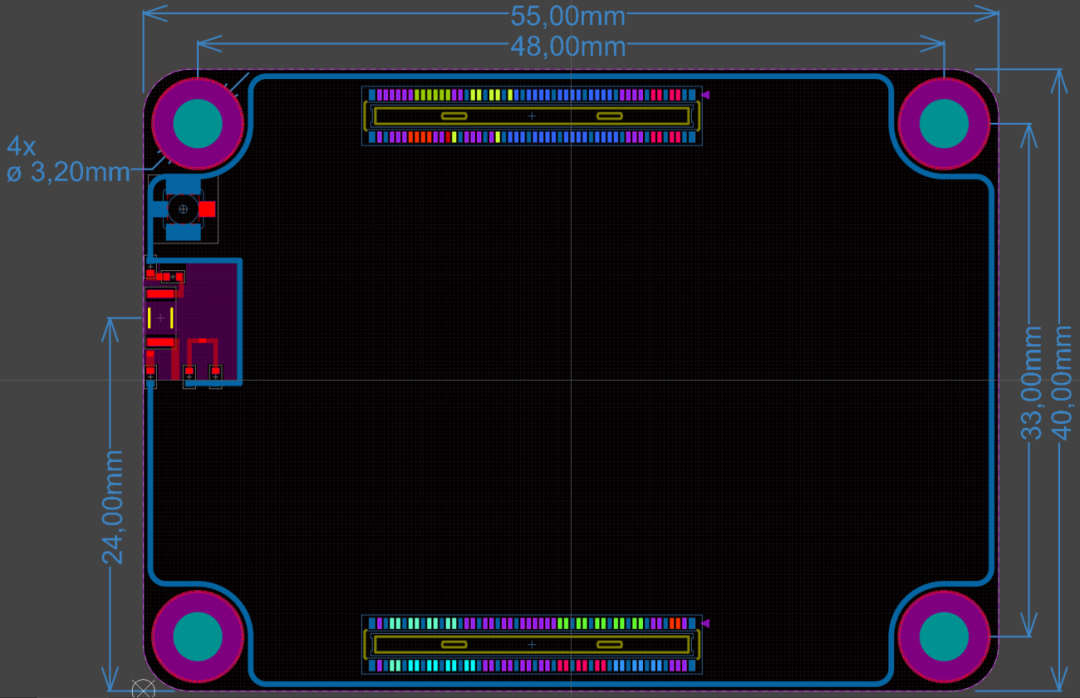
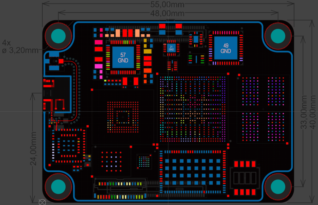
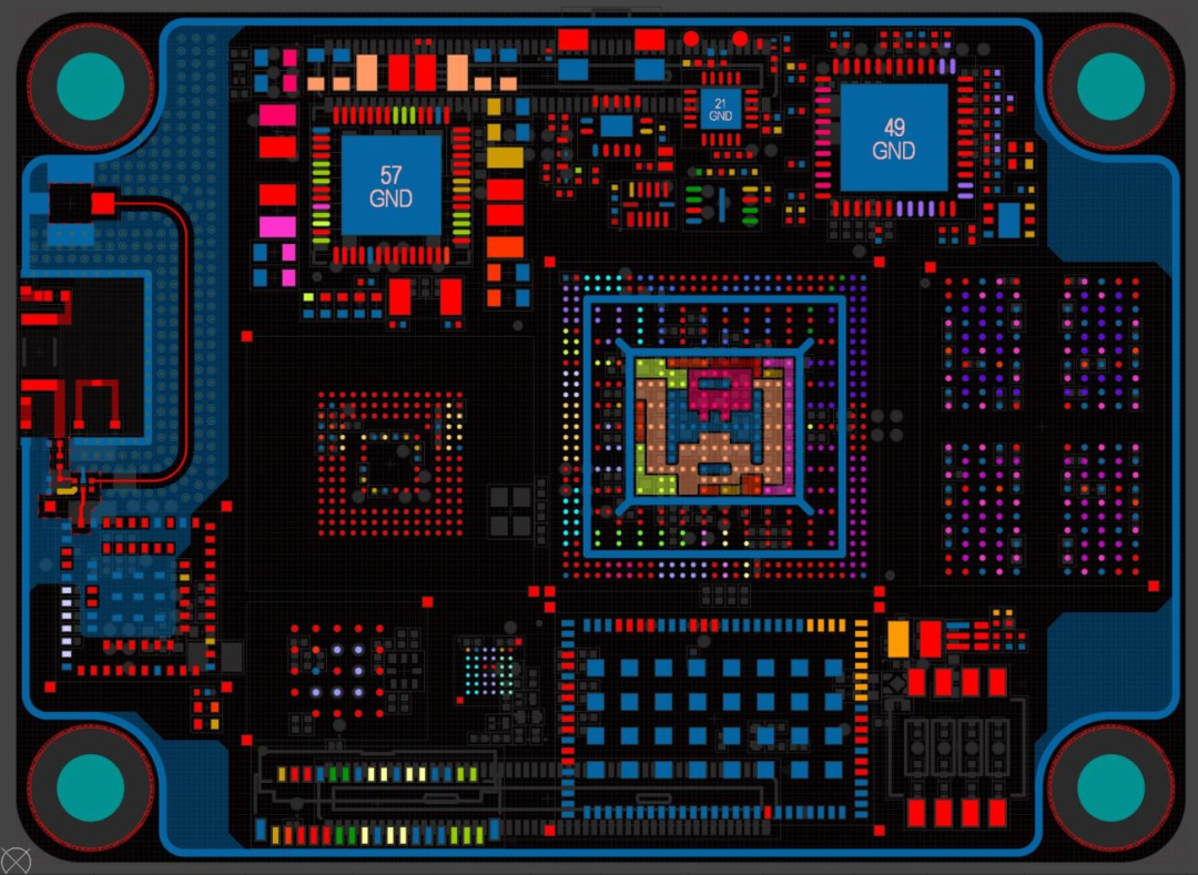
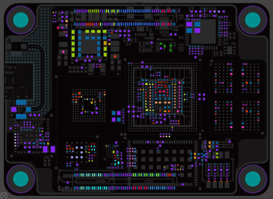
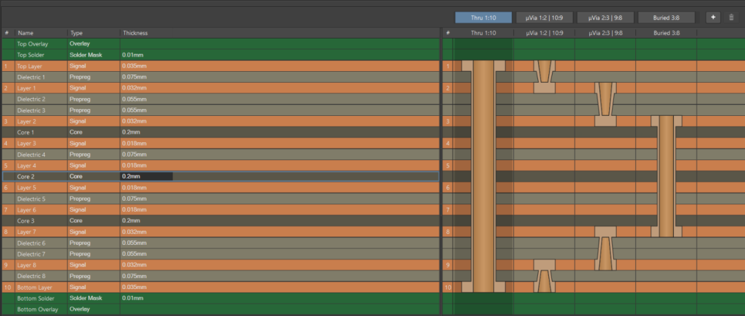
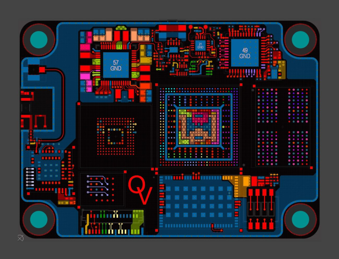
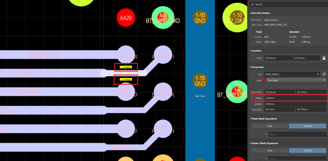
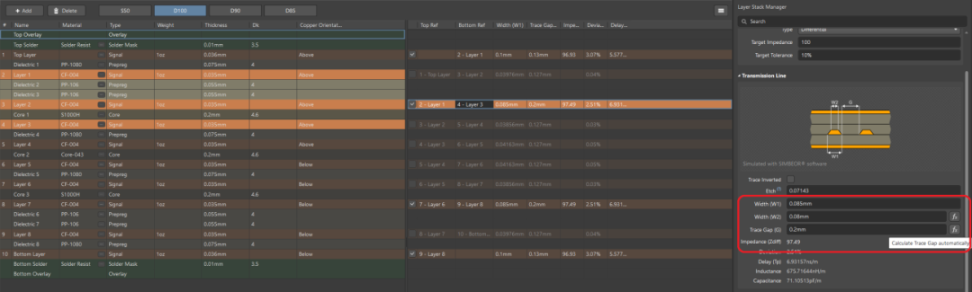
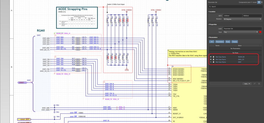
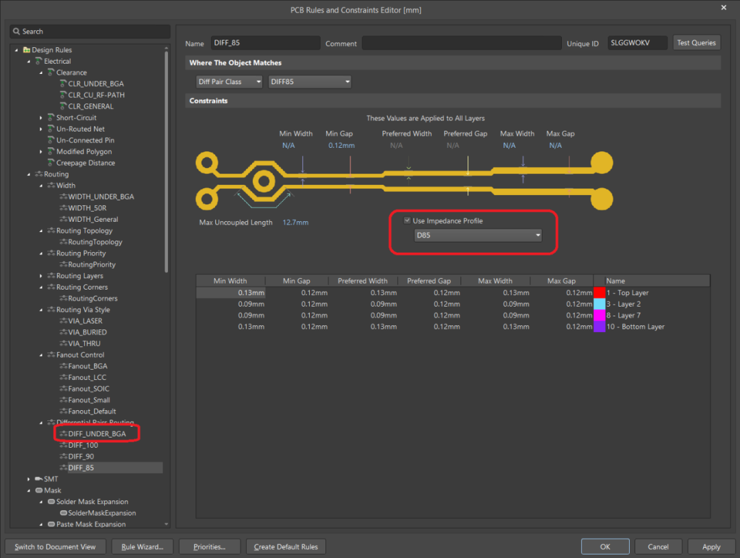
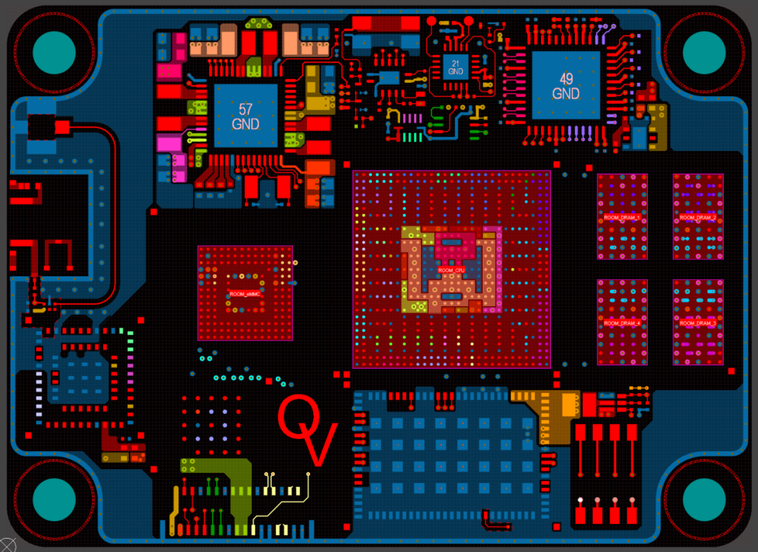
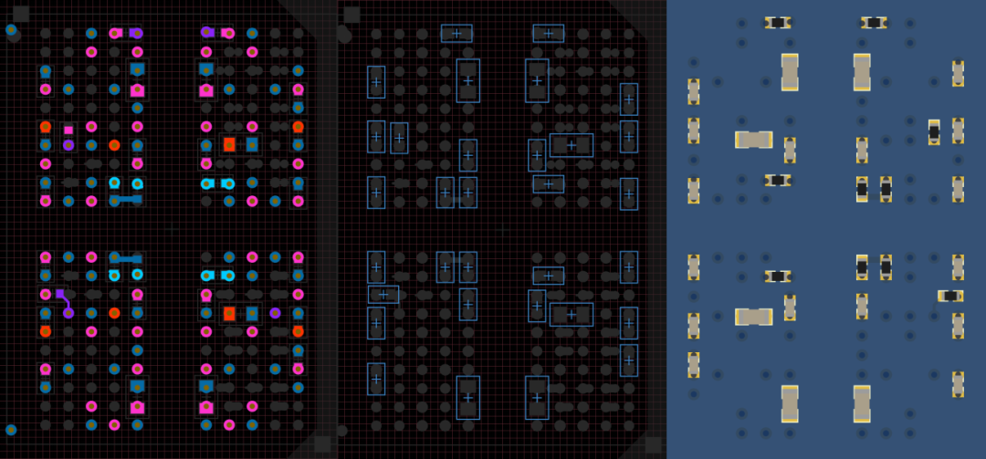
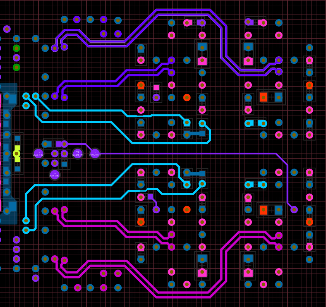
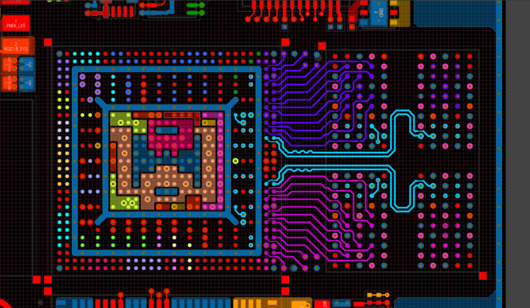
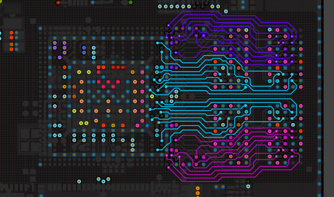
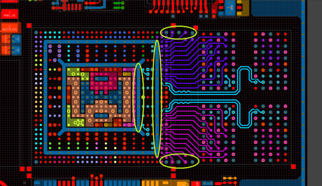
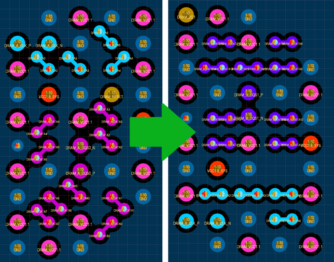
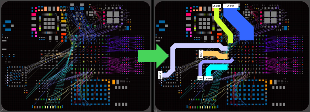
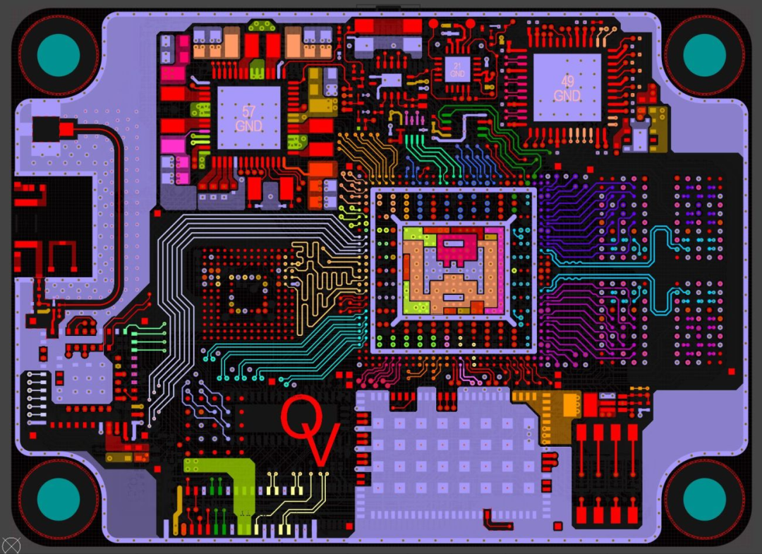
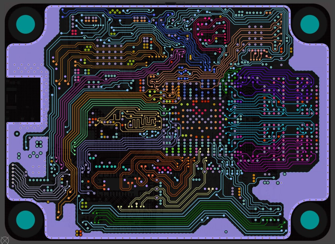
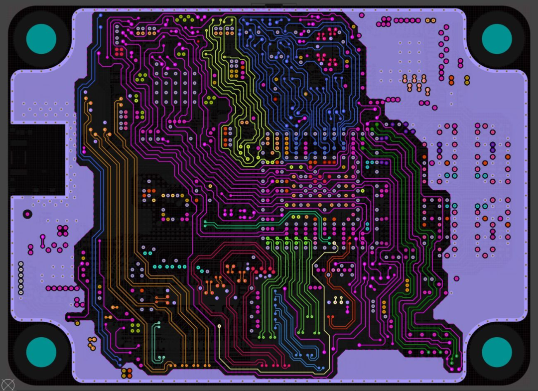
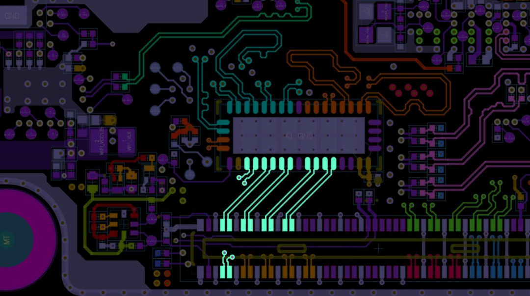
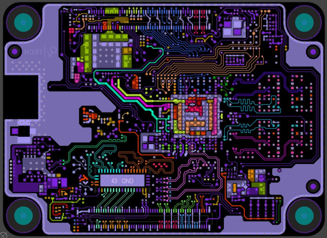
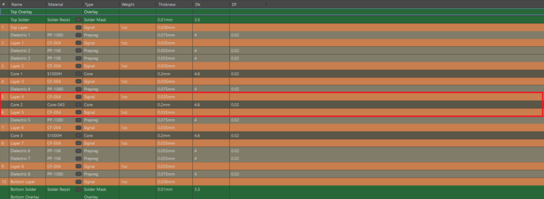
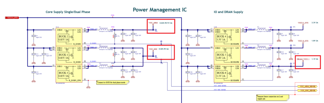
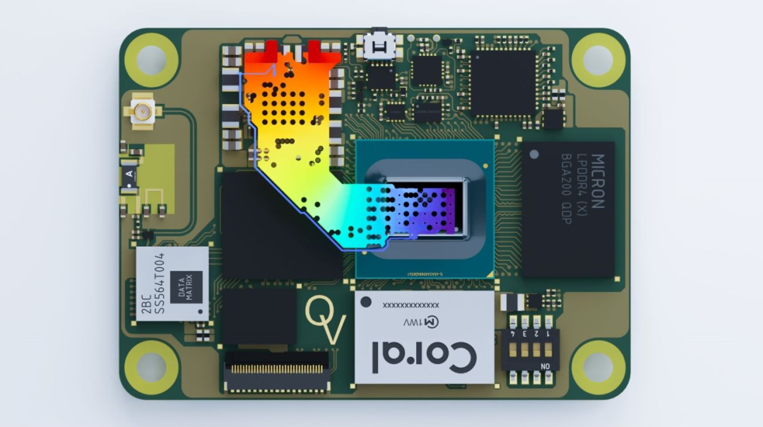
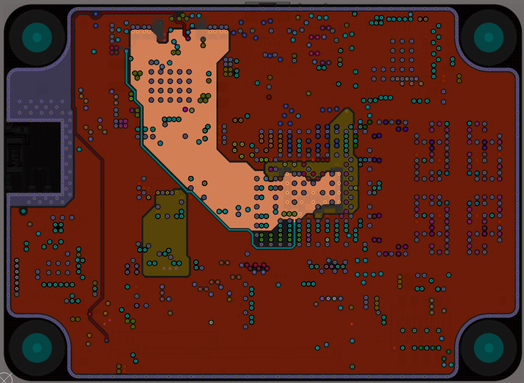
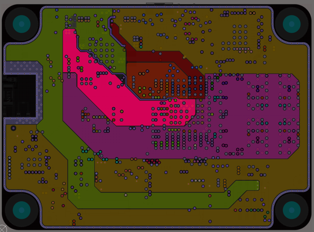
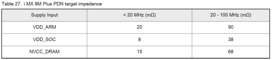
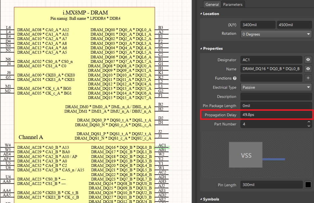
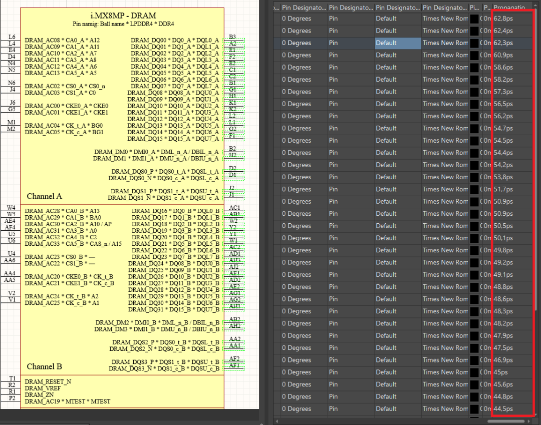
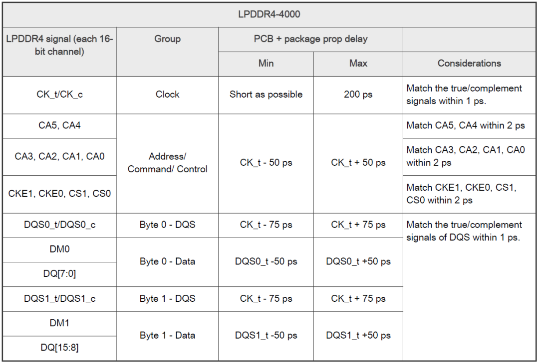
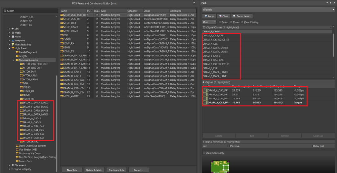
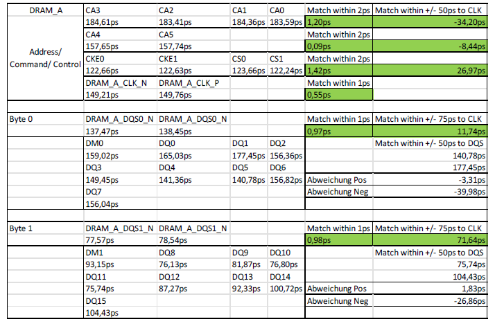
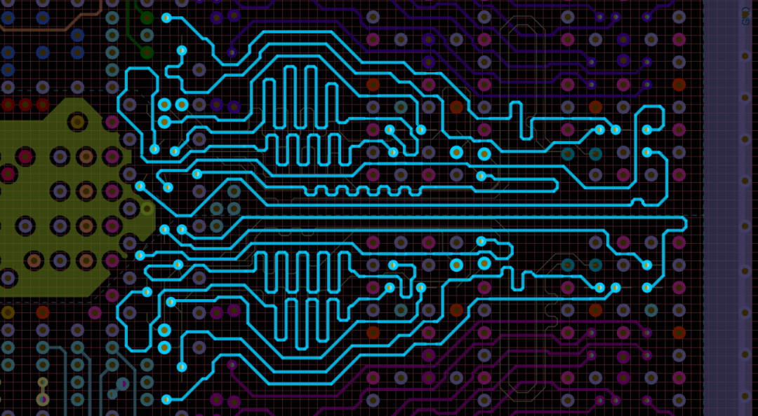
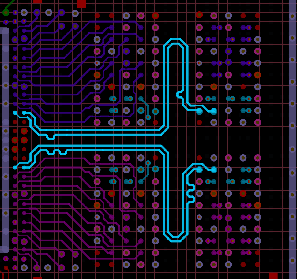
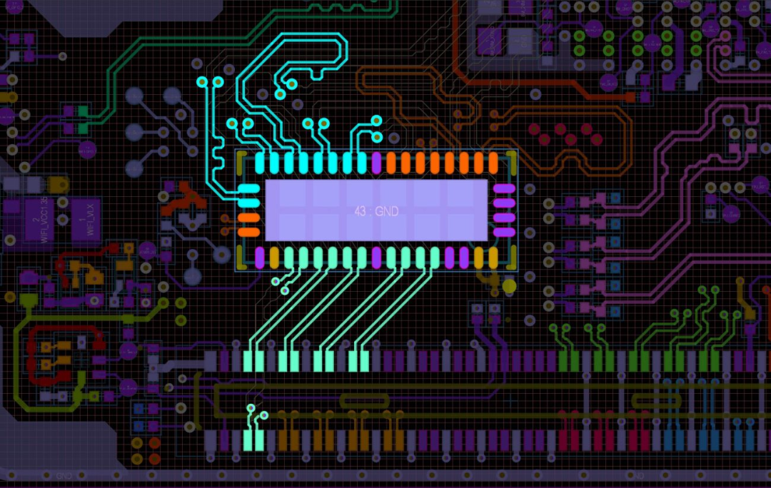
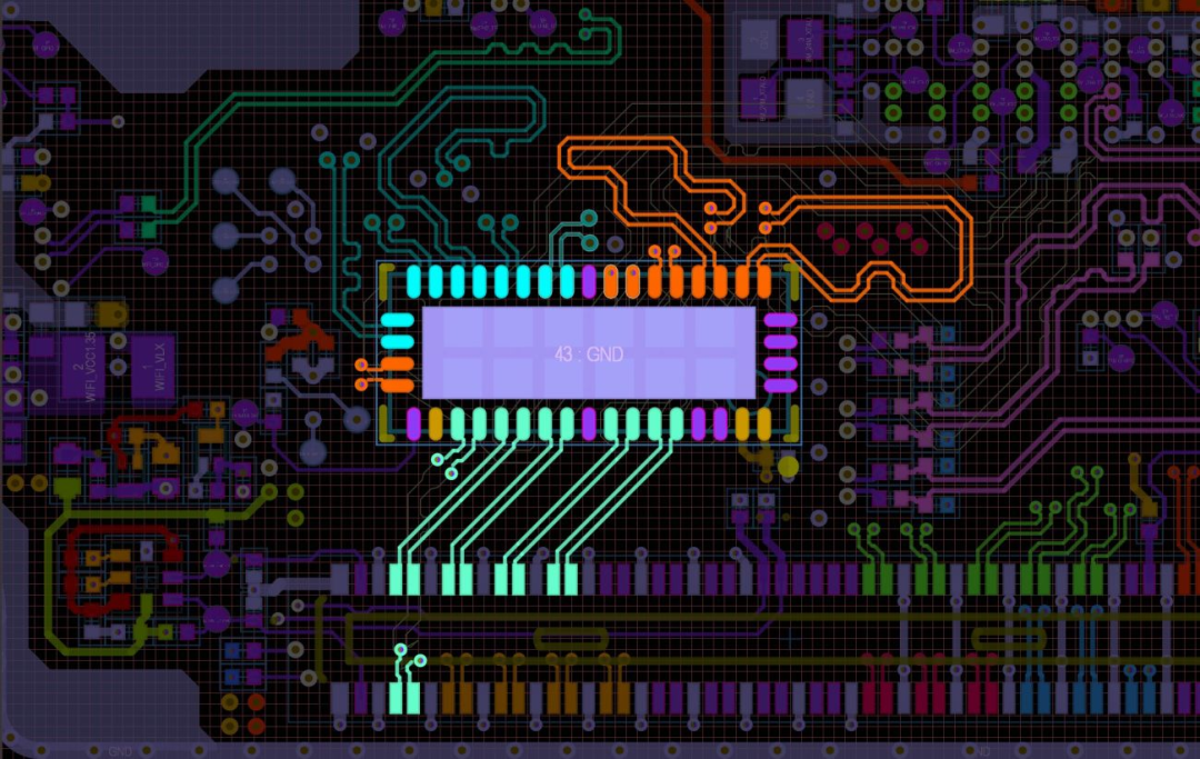
前几天在AD官网看到一个非常好的PCB设计案例,一点不夸张!布局真的让人一眼就爱上。发布之后先后有四五个人问过我,其中不乏PCB专家级的老师也觉得很规范,很优美。抱着欣赏的态度,我把关键的PCB高清图整理了下来,为保持原汁原味,我把每一步的关键词都保留了原来英文的注解。以下供大家欣赏&&解压。Image of the previous Pi.MX8 layout revisionTest-fitting the key componentsMechanical dimensions and connector locations of the PCBPositioning of mounting holes and connectors on the PCBDefining the antenna locationPCB with guard ringPreliminary placement of the key componentsComponent placement top sideComponent placement bottom sidePi.MX8 LayerstackBreak-out routing on the top layer of the moduleTrace width and spacing requirements for the i.MX8 break-out routingLayerstack manager impedance profile differential 100 OhmMultiple net classes assigned to a design blanketImpedance profile used in the design rule dialog–high priority rule overrides impedance profileDesign rooms in red shown underneath fine-pitch BGAsDecoupling capacitors placed on bottom side of the LPDDR4 ICDRAM routing bottom sideDRAM top side routingDRAM L2 routingReturn path VIAs for the DRAM interfaceReturn path management - voids and splits on the left side, improved routing on the right side Layout planning in Inkscape with an Altium Designer screenshot as a background imageTop layer routing of the PiMX8 moduleRouting inner signal layer 1Routing inner signal layer 2Multiplexer pinout with one long line in the interfaceBottom layer routing PiMX8 moduleAvailable power plane layersPMIC core and memory supply for the SoCVoltage drop across power polygonVCC_SOC polygonVCC_ARM highlighted and DRAM power rail in purplePower rails target impedancePin package delay in the schematic symbolPin delays in table format through the SCHLIB List toolbarLPDDR4-4000 PCB delay tuning requirementsX-signal classes for the LPDDR4 tuningDelay tuning documentation in ExcelDelay tuning address/command/control linesClock delay tuning top layerLVDS routed to the multiplexerMIPI-DSI routed to the multiplexer“要好好工作,但是请不要把把所有赌注压在公司”,多提升自己,也欢迎各位同学购买我们整理的优质硬件设计资料: