芯片封装的热设计

翻译自瑞萨电子官网,供学习参考,欢迎交流~
Thermal Design for Packages | Renesas --- 封装热设计 | Renesas
Lower thermal resistance enables the devices perform consistently and ensures lifetimes, helping meet market needs for higher performance as well as saving costs by curtailing the need for heat dissipation measures.
较低的热阻使器件性能一致并确保使用寿命,有助于满足市场对更高性能的需求,并通过减少对散热措施的需求来节省成本。
This article introduces various actions that can be taken to lower the thermal resistance of a package, taking two representative package types, QFP and BGA, as examples.
本文以两种代表性的封装类型QFP和BGA为例,介绍了可以采取的降低封装热阻的各种措施。
Lowering Thermal Resistance of QFPs
降低QFP的热阻
Renesas Electronics Co. offers various QFP types shown in the diagram below to meet power-consumption requirements of devices. QFPs with built-in heat spreaders have been produced for decades for devices that consume larger power. In response to increasing power consumption of devices, QFPs with exposed die pads (HQFP) have been lined up (see below). Soldering the exposed die pad on a PWB will enhance its thermal conductivity (see diagram below). For smaller pin count range, where smaller package size is required, full variations of QFNs are available. They also have exposed die pads; therefore, soldering the pads is beneficial to enhance the thermal conductivity as well.
瑞萨电子有限公司提供下图所示的各种QFP类型,以满足设备的功耗要求。具有内置散热器的qfp已经生产了几十年,用于消耗更大功率的设备。响应于器件功耗的增加,具有暴露的管芯焊盘 (HQFP) 的qfp已经被排列 (见下文)。在PWB上焊接暴露的管芯焊盘将增强其导热性 (见下图)。对于较小的引脚数范围,需要较小的封装尺寸,可以使用qfn的完整变体。它们还具有暴露的管芯焊盘; 因此,焊接焊盘也有利于增强热导率。
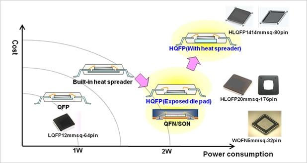
Figure 5 Thermally enhanced QFP variations
图5热增强QFP变化
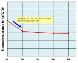
Figure 6 Ratio of soldered area to the exposed die pad area (%)
图6焊接面积与暴露的管芯焊盘面积之比 (%)
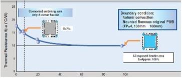
Figure 7 Ratio of soldered area to the heat spreader area (%)
图7焊接面积与散热器面积之比 (%)
Lowering Thermal Resistance of BGA
降低BGA的热阻
The thermal resistance of BGAs can be lowered by addressing four aspects: thermal balls, higher layer count of substrate,metal core design and PWB design.
可以通过解决以下四个方面来降低bga的热阻: 热球,较高的衬底层数,金属芯设计和PWB设计。
Use of thermal balls as a low-cost solution
使用热球作为低成本解决方案
In terms of package structure, a heat dissipation path is secured from the rear side of the chip to the solder balls immediately beneath the chip by providing a large number of solder balls on the rear side of the chip and thermally connecting these solder balls to the die pad via through-holes (thermal vias). These balls at the center of a package are electrically grounded and commonly called "thermal balls" as they play a thermal dissipation role by conducting heat to the PWB.
在包装结构方面,通过在芯片的背面上提供大量的焊球并通过通孔 (热通路) 将这些焊球热连接到管芯焊盘,从芯片的背面到芯片正下方的焊球固定散热路径。在封装的中心处的这些球是电接地的并且通常被称为 “热球”,因为它们通过将热传导到PWB而起到散热作用。
This is the cheapest way to dissipate heat. The thermal balls also serve as ground pins and neighboring balls can be assigned as signal pins, meaning that the actual number of pins can be increased.
这是最便宜的散热方式。热球还用作接地引脚,并且相邻的球可以被分配为信号引脚,这意味着引脚的实际数量可以增加。
Use of two inner layers of package substrate as ground layers
使用封装基板的两个内层作为接地层
Generally, a having four or more layers, including power and ground layers, is used as the package substrate for BGAs to ensure satisfactory electrical characteristics. Recently, however, the use of a 4-layer structure to lower the thermal resistance, rather than improve electrical characteristics, has been increasing.
通常,具有四层或更多层 (包括电源和接地层) 的a被用作BGAs的封装基板,以确保令人满意的电特性。然而,近来,越来越多地使用4层结构来降低热阻,而不是改善电特性。
In this case, heat from the chip is transmitted to the inner layers via the die pad's through-holes, which also serve as grounds, and two out of the four inner layers are used as grounds to secure a heat dissipation path.
在这种情况下,来自芯片的热经由也用作接地的管芯焊盘的通孔传递到内层,并且四个内层中的两个用作接地以确保散热路径。
To further decrease thermal resistance, a substrate with a thick embedded metal core layer is used.
为了进一步降低热阻,使用具有厚的嵌入金属芯层的衬底。
Use of embedded heat spreader
使用嵌入式散热器
If the combination of thermal balls and a 4-layer package substrate still fails to satisfy the thermal resistance requirement, a heat spreader can be embedded in the package. Such a heat spreader serves to diffuse the heat transmitted through the mold resin to the surface of the package. However, the reduction in thermal resistance that can be achieved this way is limited because the heat spreader is not in direct contact with the die pad and the chip.
如果热球和4层封装基板的组合仍然不能满足热阻要求,则可以在封装中嵌入散热器。这种散热器用于将通过模制树脂传递的热量扩散到封装的表面。然而,可以通过这种方式实现的热阻的减小是有限的,因为散热器不与管芯焊盘和芯片直接接触。
PWB designPWB设计
The thermal resistance of a BGA is significantly affected by the PWB design, such as the number of thermal via holes, the number of PWB layers, and the occupancy rate of Cu-trances on the PWB surface. Reassessment of the thermal design of the entire system would offer a low-cost solution that meets thermal resistance requirements.
BGA的热阻受PWB设计的显着影响,例如热通孔的数量,PWB层的数量以及PWB表面上Cu的占有率。重新评估整个系统的热设计将提供满足热阻要求的低成本解决方案。
The picture below shows examples of measureshow to lower the thermal resistances of BGAs.
下图显示了如何降低bga热阻的措施示例。
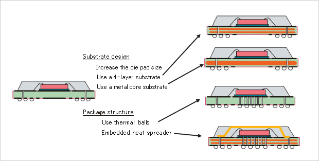
Figure 8 Low Thermal Resistance Design of BGAs
图8 bga的低热阻设计
Measuring the Junction Temperature of a Device is also Important.
测量器件的结温也很重要。
Measuring the temperature of the chip after it has been installed in a system may be considered pointless because the package has already been selected at that stage. Nevertheless, such measurement data are useful for estimating the power consumption of devices to be developed in the future. Furthermore, if the power consumption of the system is known to be considerably above the value estimated at the design phase, it is very important to know the junction temperature of the device under actual use in the system.
在将芯片安装在系统中之后测量芯片的温度可能被认为是没有意义的,因为在该阶段已经选择了封装。然而,这样的测量数据对于估计将来要开发的设备的功耗是有用的。此外,如果已知系统的功耗大大高于在设计阶段估计的值,则知道系统中实际使用的器件的结温是非常重要的。